4. Sequential Logic
Feel free to use your laptop
You are strongly encourage to work with others
When you get stuck, ask those sitting around you for help
Get used to working together in the labs
Peer teaching and peer learning has been empirically shown to be very effective
For these questions, feel free to use a single Digital workspace for all the circuits. However, label each circuit with labelled rectangles. These are components that can be found under Components -> Misc. -> Decoration -> Rectangle.
Where possible, each question should have complete tests. The test component can be found under Components -> Misc. -> Test case. Once a test component is placed on the workspace, right click on the component to edit the test data.
Questions may have restrictions on the logic gates that may be used. When restrictions are stated, they only apply to the gates; inputs, outputs, wires, etc. may be still be used.
4.1. Latches & Flip-Flops
Create a S-R Latch
Play with the circuit enough to become comfortable with all possible states and inputs
Do not forget to include tests for all circuits
Create a D latch
Simplify the circuit by eliminating the \(\lnot Q\) output
Play with the circuit enough to become comfortable with all possible states and inputs
Create a D latch with Enable
Add a “Data Graph” component to the design
Can be found under Components -> IO -> Data Graph
Play with the circuit enough to become comfortable with all possible states and inputs
Create a D flip-flop
Add a new output component between the output of the first D latch and the second
Be sure to label this component
Read the Test component’s help to learn how to handle the clock input
Right click the Test component -> Edit -> Help
Be sure to include the new labelled output component to the tests
4.2. Registers
Create a 1 bit register using a D flip-flop component and a multiplexer
This is the same design seen in lecture
Using the design from above, create an 8 bit register
Create 8 copies of the 1 bit register
This is the same configuration seen in lecture
Modify the above design to provide control over when the register outputs data
Currently the \(EN\) signal controls when data is written to the register
Rename this component \(EN_{i}\)
A signal \(EN_{o}\) is to be added to control when the output of the register reaches the output components
HINT: Use a driver component
Component -> Wires -> Driver
Refer to the Test component’s help to learn how to handle high impedance state
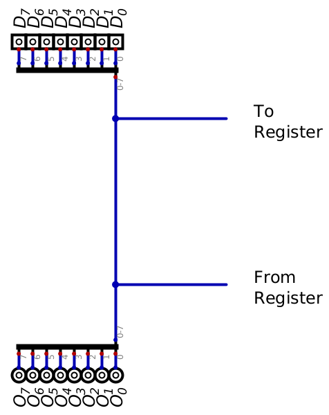
Modify the above design to have the register’s input and final output on the same signal lines
You will need to alter the Input components to be tri-state
Right click on an Input component -> Advanced tab -> toggle “Is three-state input”
Refer to the following figure for an example of what this may look like
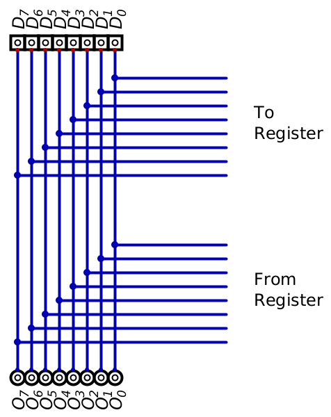
Simplify the above design by replacing the D flip-flop/mux 1 bit registers with a single 8 bit register component
Components -> Memory -> Register
Right click the register component to modify the number of data bits it has
This design requires the signal lines to carry multiple bits
Refer to the following figure for an example of what this may look like