19. Control Logic
Instructions are fetched and put into the instruction register for processing
An instruction set has already been defined
Each instruction’s microcodes are known
How the hardware is manipulated for each instruction
However, there is still no way for the system to manipulate its own control logic
There is no way for the system to take an instruction and then activate/deactivate the various hardware modules
In other words, how can the system know how to physically perform an instruction?
19.1. Instruction and Microcode Steps
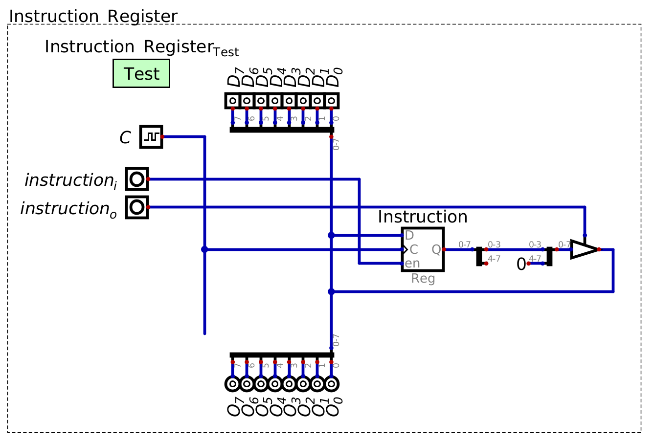
The instruction register stores the operator and operand of the current instruction. The operand is output to the bus for use during the execution of the instruction. The operator remains in the register for processing.
Consider what is stored in the instruction register and what is being output
The operator, specifying some instruction to execute
The most significant four bits in the instruction
The operand, specifying some data for use in execution of the specific instruction
The least significant four bits in the instruction
As previously discussed, each instruction requires several steps
For example, loading data into register A from RAM (
LDAR/0001)Output the operand from the instruction register and put it into the address register
Output the value from the specified RAM address to the A register
Additionally, before any processing of any instruction can occur, it must be fetched from RAM
No matter what instruction is to be executed, the two steps in the fetch cycle must happen
In other words, instructions require several steps
19.1.1. Microcode Counter
The operator can be used to specify the steps to be executed in order to perform the instruction
The operator would manipulate the control signals for the system
Thus, a look up table can be used to find the steps required to perform the full instruction
Input to the look up table is the operand, output is the control signals
However, there is a problem with this idea since instruction may require several sequential steps too complete
The microcodes
Consider the below table of the 4 microcode steps required for loading data from RAM to register A
The first two steps are the fetch cycle
The latter two steps move dara from the specified RAM address to register A
\(Address\) |
\(RAM\) |
\(A\) |
\(B\) |
\(ALU\) |
\(out\) |
\(PC\) |
\(Instruction\) |
|---|---|---|---|---|---|---|---|
|
|
|
|
|
|
|
|
|
|
|
|
|
|
|
|
|
|
|
|
|
|
|
|
|
|
|
|
|
|
|
|
Not all instructions require 4 steps
1 instruction (
NOOP) takes 2 microcode steps (fetch only)Six instructions take 3 steps
Six instructions take 4 steps
For simplicity and consistency, consider each instruction as a group of 4 steps
Below is a table of the microcode steps of the first 3 instructions in the instruction set
NOOPLDARLDAD
Operator |
Microcode Step |
Control Logic |
|
|---|---|---|---|
|
|
Program Counter -> Address Register |
|
|
|
RAM -> Instruction Register, Enable Program Counter |
|
|
|
Nothing |
|
|
|
Nothing |
|
|
|
Program Counter -> Address Register |
|
|
|
RAM -> Instruction Register, Enable Program Counter |
|
|
|
Instruction Register -> Address Register |
|
|
|
RAM -> Register A |
|
|
|
Program Counter -> Address Register |
|
|
|
RAM -> Instruction Register, Enable Program Counter |
|
|
|
Instruction Register -> Register A |
|
|
|
Nothing |
|
… |
… |
… |
Each operator specifies a grouping of microcodes
Each microcode can be identified by the microcode step count
Considering the operand and microcode step together, there is a unique identifier for each instruction’s microcode
A unique six bit identifier
Four bits for the operator, two for the microcode step
Therefore, given a mechanism to keep track of the microcode step, a look up table may still be used
Map the operand + microcode counter to the control logic for the specific microcode step
Fortunately, there is a simple way to keep track of the microcode steps — a counter
Like the program counter
This counter will be referred to as the microcode counter
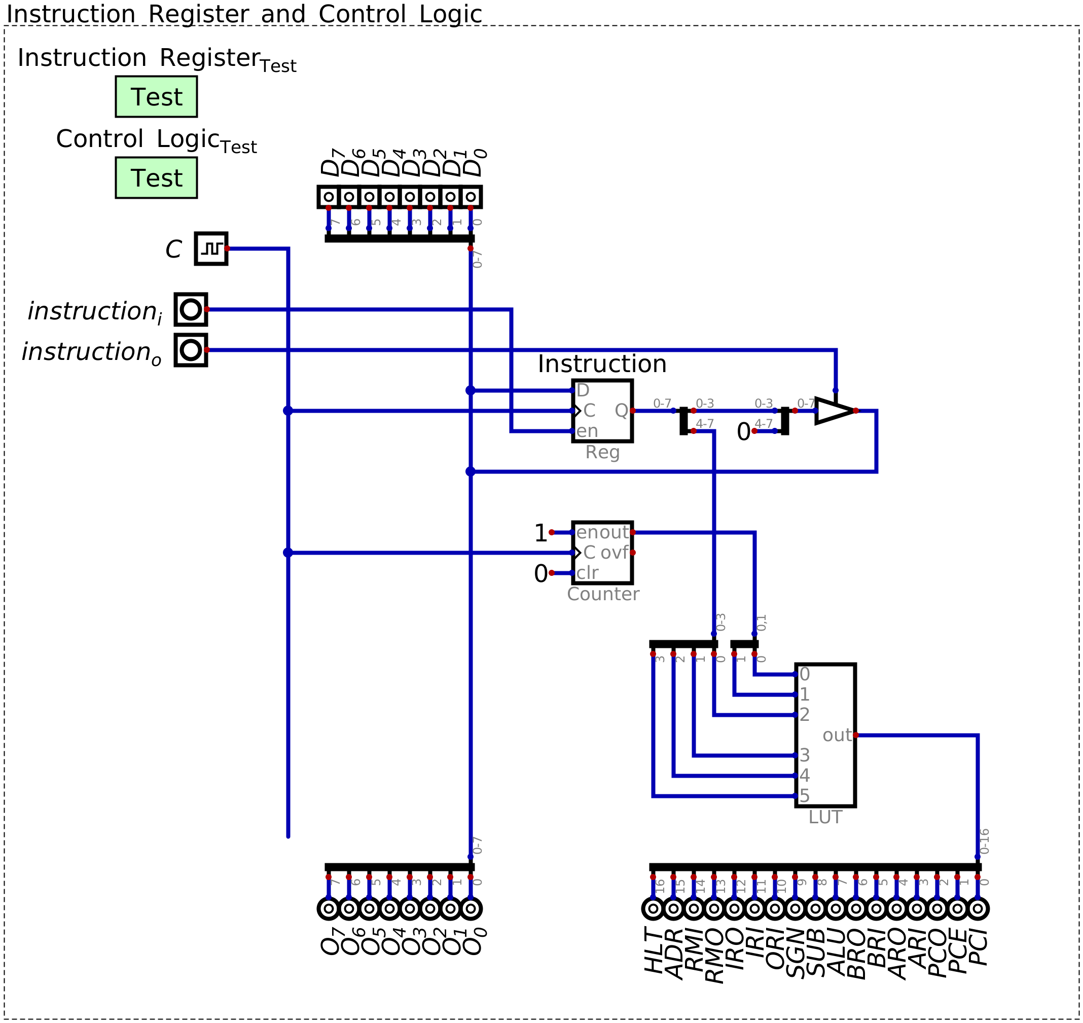
Operator from the instruction register and microcode step count from the microcode counter used as input to a look up table containing the control signals. The input to the look up table would map to the control signals for the specific operator’s current microcode step.
Unlike the program counter, this microcode counter will count at every clock pulse
The program counter only counted when enabled since each individual instruction may take several clock pulses
The microcode counter keeps track of each microcode step, each taking one clock pulse
Note
Since several instructions takes less than four clock cycles, one may have noticed that the system would be wasting clock cycles; the system would be doing nothing for a clock pulse. What are some ways this could be addressed?
19.2. Look Up Table to Process Instruction
Given the 16 instructions, each with 4 microcode steps, there are a total of 64 rows in the look up table
Each of these rows contains binary patterns controlling many control signals
One could write out the look up table by hand, but this would be tedious
Therefore, a script will be create to programmatically generate the hex file for the look up table
Similar to how it was done for the seven segment display patterns
With the current configuration of the ESAP system, a total of 17 control signals exist
Therefore, the look up table will have a 17 bit output where each bit corresponds to a specific control signal
Below is a series of constants labelling each of the 17 bits
36HLT = 0b1_00000000_00000000
37ADR = 0b0_10000000_00000000
38RMI = 0b0_01000000_00000000
39RMO = 0b0_00100000_00000000
40IRO = 0b0_00010000_00000000
41IRI = 0b0_00001000_00000000
42ORI = 0b0_00000100_00000000
43SGN = 0b0_00000010_00000000
44SUB = 0b0_00000001_00000000
45ALU = 0b0_00000000_10000000
46BRO = 0b0_00000000_01000000
47BRI = 0b0_00000000_00100000
48ARO = 0b0_00000000_00010000
49ARI = 0b0_00000000_00001000
50PCO = 0b0_00000000_00000100
51PCE = 0b0_00000000_00000010
52PCI = 0b0_00000000_00000001
Here, the most significant bit of the 17 output bits controls the \(Halt\) signal
\(Halt\) has yet to be discussed, but will deactivate the system’s clock, thereby halting the program
The least significant bit controls the \(PC_{i}\) signal
The actual order of these signals does not really matter
The fact that \(Halt\) is the most significant bit is by no means necessary
All that matters is that each signal connects to the corresponding module in the ESAP system
Here, the order is set for visual clarity and symmetry of the control bus
With these constants set, one can easily create microcodes by performing bitwise
ORon the constantsFor example, to create the microcode for “Instruction Register -> Address Register” —
IRO|ADRThis creates the full 17 bit binary pattern to activate the corresponding modules for the microcode
IRO|ADR0_00010000_00000000 | 0_10000000_000000000_10010000_00000000
Each of the 16 instructions will be a collection of up to 4 groups of specific constants
ORed togetherBelow, the instructions are stored in a list of 16 lists of length 4
Each list of length 4 corresponds to the 4 microcodes for a specific instruction
Each of the 16 lists of length 4 corresponds to a specific instruction
60INSTRUCTIONS = [
61    [PCO|ADR,   RMO|IRI|PCE, 0,           0           ],  # 0b0000 --- 0x0 --- NOOP --- No Operation
62    [PCO|ADR,   RMO|IRI|PCE, IRO|ADR,     RMO|ARI     ],  # 0b0001 --- 0x1 --- LDAR --- Load A From RAM
63    [PCO|ADR,   RMO|IRI|PCE, IRO|ARI,     0           ],  # 0b0010 --- 0x2 --- LDAD --- Load A Direct
64    [PCO|ADR,   RMO|IRI|PCE, IRO|ADR,     RMO|BRI     ],  # 0b0011 --- 0x3 --- LDBR --- Load B From RAM
65    [PCO|ADR,   RMO|IRI|PCE, IRO|BRI,     0           ],  # 0b0100 --- 0x4 --- LDBD --- Load B Direct
66    [PCO|ADR,   RMO|IRI|PCE, IRO|ADR,     ARO|RMI     ],  # 0b0101 --- 0x5 --- SAVA --- Save A to RAM
67    [PCO|ADR,   RMO|IRI|PCE, IRO|ADR,     BRO|RMI     ],  # 0b0110 --- 0x6 --- SAVB --- Save B to RAM
68    [PCO|ADR,   RMO|IRI|PCE, ALU|ARI,     0           ],  # 0b0111 --- 0x7 --- ADAB --- Add B to A
69    [PCO|ADR,   RMO|IRI|PCE, ALU|SUB|ARI, 0           ],  # 0b1000 --- 0x8 --- SUAB --- Subtract B from A
70    [PCO|ADR,   RMO|IRI|PCE, IRO|PCI,     0           ],  # 0b1001 --- 0x9 --- JMPA --- Jump Always
71    [PCO|ADR,   RMO|IRI|PCE, 0,           0           ],  # 0b1010 --- 0xA --- NOOP --- No Operation
72    [PCO|ADR,   RMO|IRI|PCE, 0,           0           ],  # 0b1011 --- 0xB --- NOOP --- No Operation
73    [PCO|ADR,   RMO|IRI|PCE, 0,           0           ],  # 0b1100 --- 0xC --- NOOP --- No Operation
74    [PCO|ADR,   RMO|IRI|PCE, IRO|ADR,     RMO|ORI     ],  # 0b1101 --- 0xD --- OUTU --- Output Unsigned Integer
75    [PCO|ADR,   RMO|IRI|PCE, IRO|ADR,     RMO|ORI|SGN ],  # 0b1110 --- 0xE --- OUTS --- Output Signed Integer
76    [PCO|ADR,   RMO|IRI|PCE, HLT,         0           ],  # 0b1111 --- 0xF --- HALT --- Halt
77]
Notice that each of the 16 instructions start with the same two microcodes
PCO|ADRandRMO|IRI|PCEThese are the two microcodes of the fetch cycle
This way, no matter what operator value is in the instruction register, fetch happens the same way
With all microcodes set for each instruction, the list of instructions can be written as hex values to an output file
 99with open("control_logic_patterns_for_look_up_table.hex", "w") as hex_file:
100    hex_file.write("v2.0 raw\n")
101    for instruction in INSTRUCTIONS:
102      hex_file.writelines(f"{hex(microcode_pattern)}\n" for microcode_pattern in instruction)
This file can be loaded into the control logic’s look up table
With this, the look up table can now map the input (operator + microcode step) to the 17 bit control signal pattern
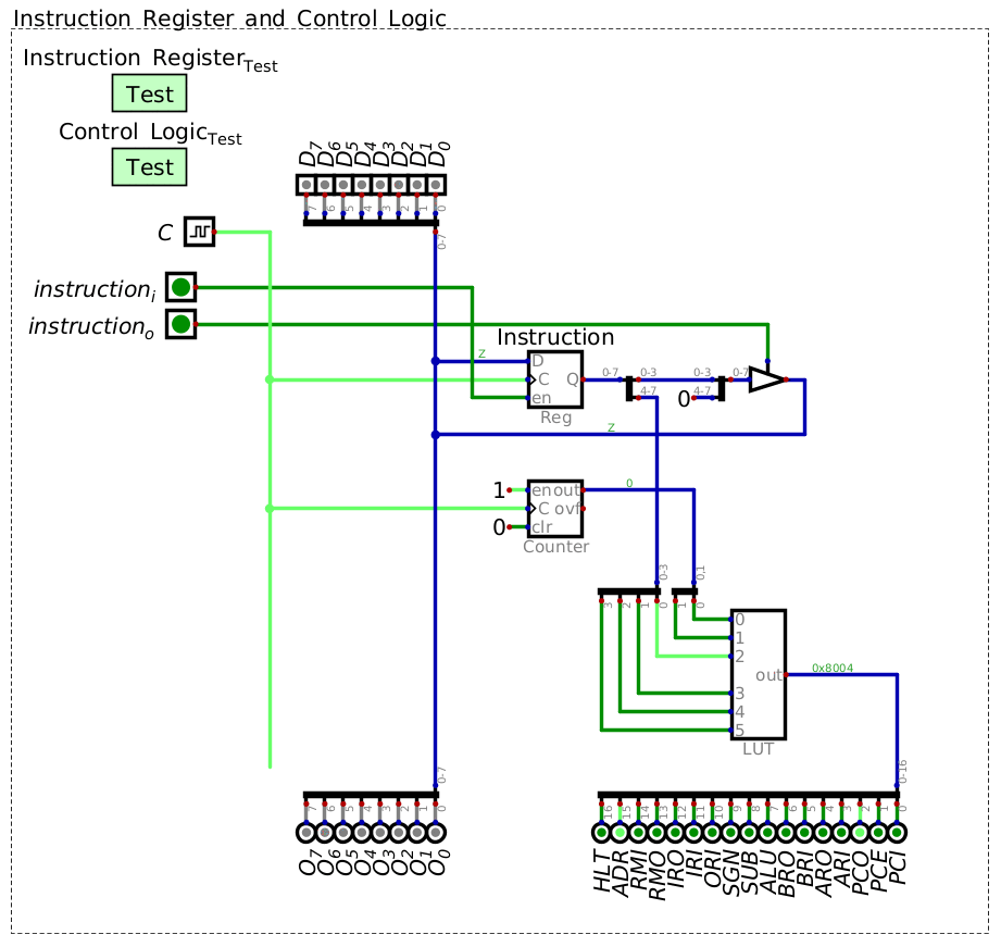
Control logic look up table outputting the 17 control signals for the four microcode steps of the instruction
0001 (LDAR).
19.3. Including the Control Logic Module in the System
Adding the control logic look up table to the system requires a reconfiguration of the control signals
The toggles for each control signal is removed as each signal is connected to the output of the look up table
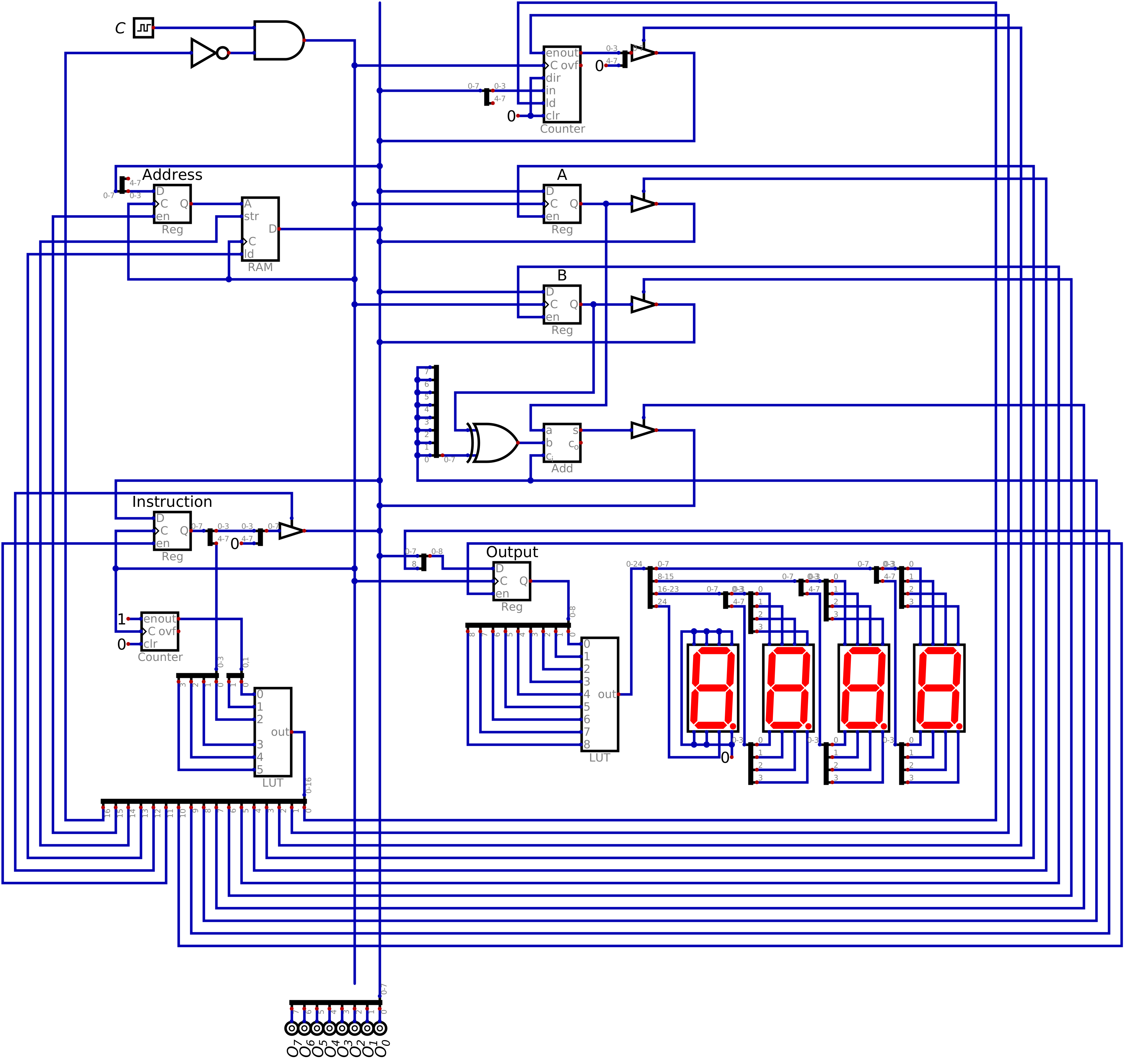
Configuration of the ESAP system with the ALU, RAM, output, program counter, instruction register and control logic modules connected.
In addition to connecting the control signals, logic was added to the system to control when the clock is active
This allows for the \(Halt\) signal to halt the system
When \(Halt\) is high, the clock is disabled
This is achieved by inverting the \(Halt\) signal and
ANDing it with the clock signal
Further, the data input toggles were removed from the top of the bus since there is no need for them anymore
All data the system needs will be programmed into RAM
There will be no need to add data to these lines while the system is running
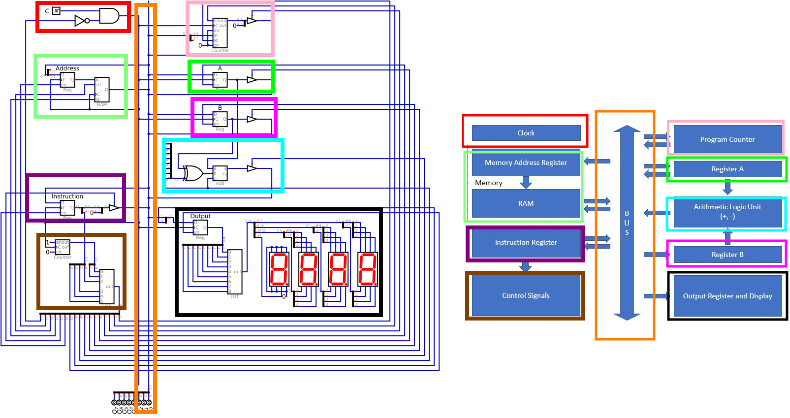
Comparison of the current system with the control logic and the ESAP architecture overview.
19.4. For Next Time
Something?