10. The Bus
The bus physically connects several components within a computer
It facilitates the transfer of information between these components, such as RAM and registers
Typically, there are three types of busses
Data bus — Transfer data between components
Address bus — Transmits memory addresses
Control bus — Sends signals responsible for controlling when components are active
10.1. Tri-State Logic
Tri-state logic was discussed in the previous topic when introducing drivers
Drivers were used to control RAM out
Briefly, components can have three different states
Output a high signal by connecting the line to some voltage source (
1)Output a low signal by connecting the line to ground (
0)High impedance state/do nothing (
Z)
For a shared signal line like a bus, it is important that only one component is outputting a value at a time
Outputting
0is not the same as outputting nothing since any other signal on the same line would be sunk to groundIn other words, if two components are connected to the same output line
If one component outputs
0by connecting the line to groundAnd the other outputs
1by connecting the line to a voltage sourceThe line would ultimately have no voltage as it would be connected to ground
As an analogy, consider a long sink with several faucets and drains connected to it
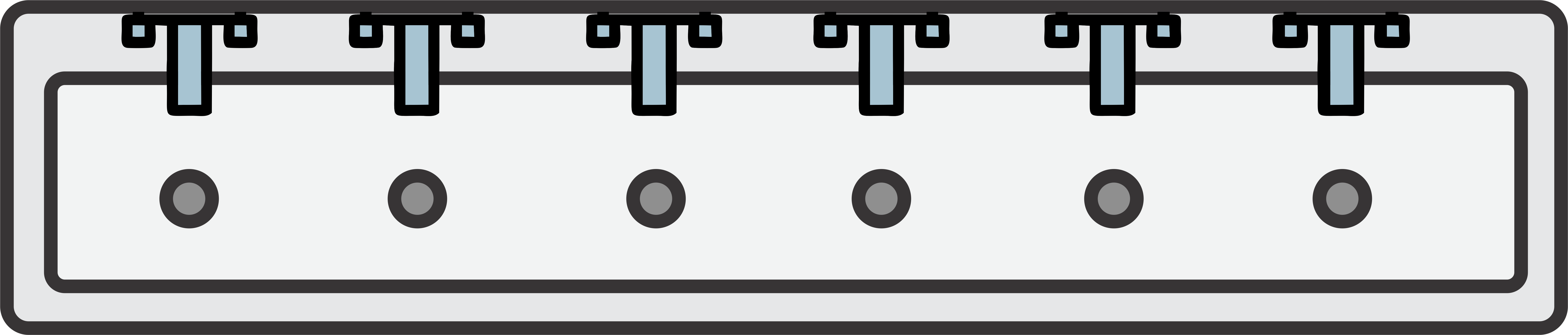
A long sink representing some signal line with several components connected. Here, the sink itself represents the line and the faucet/drain represents the component’s connection to the shared line.
Here, the sink represents some shared signal line that several components can connect to
The components’ connections to the signal line are represented by the faucets and corresponding drains
If a components is outputting a signal to the shared line, the faucet will either be on, or the drain will be open
When the output is
1, the faucet will be on adding water to the sinkWhen the output is
0, the drain will be opened, allowing any residual water to drain from the sink
All other components will be left alone (
Z), with neither the faucet on or the drains openedThe presence or absence of water in the sink means that the signal is high or low, respectively
Consider what would happen in this analogy if one tried to use
0to mean nothingIf one of the components had their faucets on, but others had their drains open, the water would immediately drain
The sink would remain empty
This would be a problem since the sink should have water in it
This is why it’s important to have a third state
10.2. Connecting Components
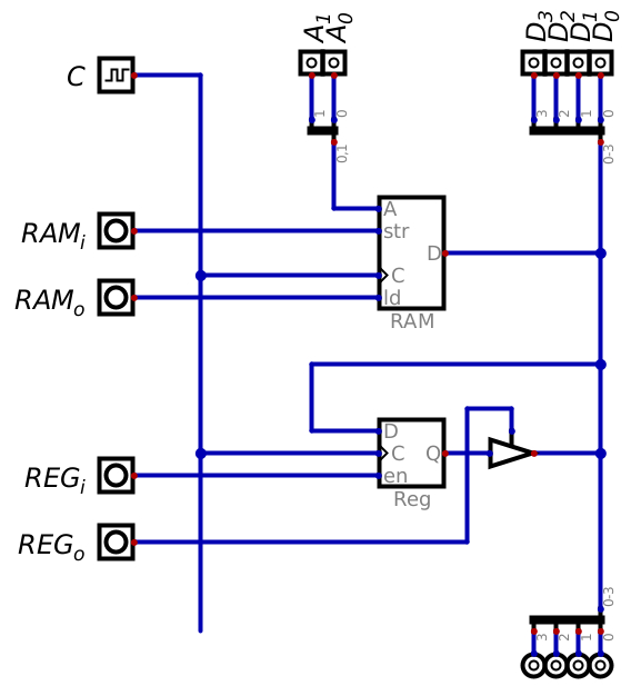
RAM and a register connected to various busses. This configuration allows for inputting data into the bus from an external source (the input buttons), controlling the memory address used in RAM, and controlling when the RAM and register components are inputting/outputting data.
Above is a RAM component connected to a register component via a data bus
With this configuration, data can be input into the system via the input buttons
The memory address the RAM component is referencing is controlled by address input buttons
Finally, the components are controlled by turning on/off their inputs and outputs
Notice how the register only has an input enable on the component
To control the register’s output, a driver is added after the register’s output
Here, how the components’ signal lines are connected is important, not the actual physical layout of the components
The location of each component in the layout is arbitrary
Within this layout are three physically separate busses
The data bus
For transferring data between components
In this configuration, there are four data lines, but more could be added
Here, data can be inputted into the system via the buttons labelled \(D_{0}\) through \(D_{3}\)
The data buttons are tri-state to provide a way to not input any value from an external source
The outputs at the bottom is there so one can see what value is on the bus at any given time
The address bus
For controlling which memory address in RAM is currently being used
Here, for simplicity, there are two address lines, meaning only four memory addresses can be accessed from RAM
These are controllable via the buttons labelled \(A_{0}\) and \(A_{1}\)
The control bus
Controls when individual components are reading from or writing to the data bus
Here, each is labeled with an \(i\) or \(o\) signifying input or output
Below is an image of the layout with the busses identified
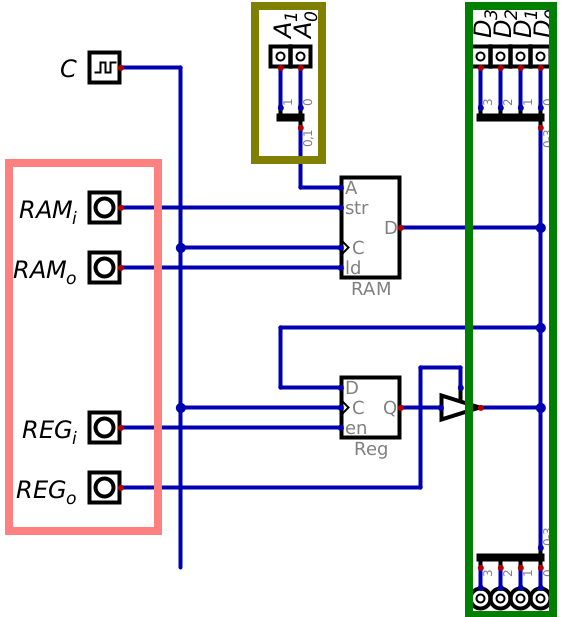
Configuration of a RAM component and a register component connected to various busses. These data bus is shown within the green box on the right, the address bus is the yellow box in the top centre, and the control bus is shown by the pink box on the left.
10.3. Loading Data into RAM
Consider how one would add data to RAM
This would require manipulating the signals along the three busses in a specific way
This is probably best explained with an example
Add the value
0001to memory address00and1000to memory address01Below is a table showing how the signals would need to be set to achieve this
This table however is not a truth table, but instead represents what is effectively a program
In the below table,
Cmeans clock pulse, which would happen only after all other signals are set
\(RM_{i}\) |
\(RM_{o}\) |
\(RG_{i}\) |
\(RG_{o}\) |
\(A_{1}\) |
\(A_{0}\) |
\(D_{3}\) |
\(D_{2}\) |
\(D_{1}\) |
\(D_{0}\) |
\(C\) |
|||
|---|---|---|---|---|---|---|---|---|---|---|---|---|---|
|
|
|
|
|
|
|
|
|
|
|
|||
|
|
|
|
|
|
|
|
|
|
|
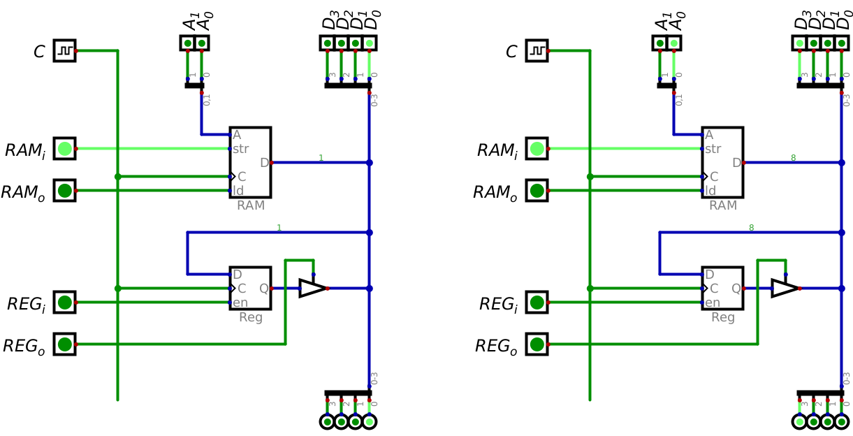
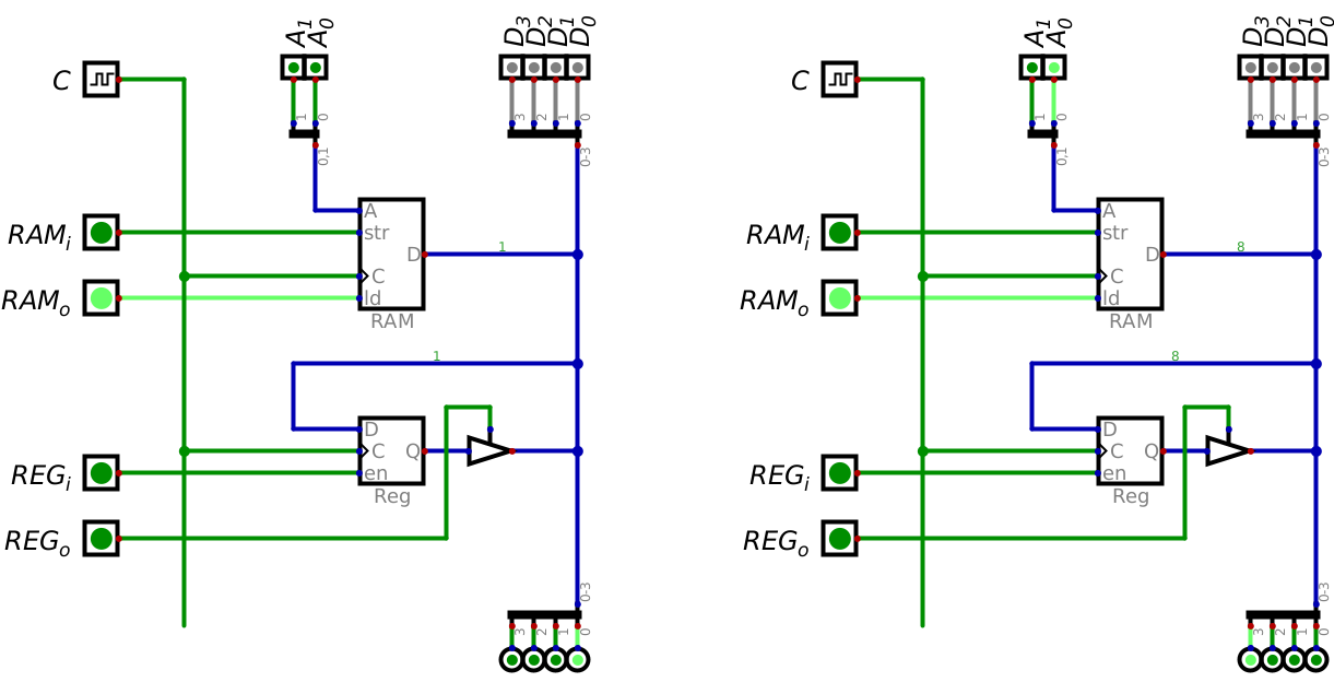
The left image shows how the signals should be set to add the value 0001 to memory address 00, and the right
shows how they should be set to add the value 1000 to memory address 01. A clock pulse would be required in
both scenarios to have the data be stored in RAM. These images correspond to the two rows in the above table.
If one wants to verify that the data did in fact get stored, a different set of signals is needed
The data stored in RAM would be displayed on the outputs at the end of the data bus
Be mindful that the data input lines need to be set to
Z, otherwise their inputs will interfere with RAM’s outputClock pulses are not actually needed here, but are included in the table for completeness
\(RM_{i}\) |
\(RM_{o}\) |
\(RG_{i}\) |
\(RG_{o}\) |
\(A_{1}\) |
\(A_{0}\) |
\(D_{3}\) |
\(D_{2}\) |
\(D_{1}\) |
\(D_{0}\) |
\(C\) |
|||
|---|---|---|---|---|---|---|---|---|---|---|---|---|---|
|
|
|
|
|
|
|
|
|
|
|
|||
|
|
|
|
|
|
|
|
|
|
|
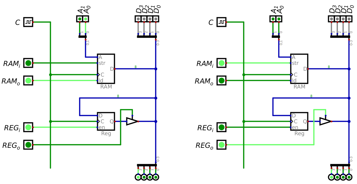
The left image shows how the signals should be set to verify that the value 0001 is stored in memory address
00, and the right shows how they should be set to verify that the value 1000 to memory address 01. These
images correspond to the two rows in the above table. The data stored in RAM at the specified memory addresses is
displayed on the output at the bottom of the data bus.
10.4. Swapping Data
Now consider a more complex problem — swap the values between the two memory addresses
Move the contents of memory address
00, which is0001to memory address01And move the contents of address
01(1000) to memory address00
Be careful to not overwrite the values in either memory address
A third, unused memory address should be used to ensure no data is lost
What would this program be?
At a high level, the solution would be
Move the value stored at memory address
00to a free address, such as10Move the value at memory address
01to00Move the value in address
10to01
However, RAM can only output or input at a clock pulse
It’s not possible to move a value between RAM addresses directly
This is where the register comes in
The register will serve as temporary storage to facilitate moving data between RAM addresses
This means the strategy to swap data would more accurately be
Move the value from memory address
00to the registerMove the value from the register to address
10Move the value at address
01to the registerMove the value from the register to address
00Move address
10's value to the registerMove the register’s value to
01
Below is a table showing the program of how the signals should be set along the busses
\(RM_{i}\) |
\(RM_{o}\) |
\(RG_{i}\) |
\(RG_{o}\) |
\(A_{1}\) |
\(A_{0}\) |
\(D_{3}\) |
\(D_{2}\) |
\(D_{1}\) |
\(D_{0}\) |
\(C\) |
|||
|---|---|---|---|---|---|---|---|---|---|---|---|---|---|
|
|
|
|
|
|
|
|
|
|
|
|||
|
|
|
|
|
|
|
|
|
|
|
|||
|
|
|
|
|
|
|
|
|
|
|
|||
|
|
|
|
|
|
|
|
|
|
|
|||
|
|
|
|
|
|
|
|
|
|
|
|||
|
|
|
|
|
|
|
|
|
|
|

The left image shows how the signals should be set for moving the contents of memory address 00 to the register.
The right shows how they should be set to move the contents of the register to memory address 10. These two
images correspond to the first two rows in the above table.
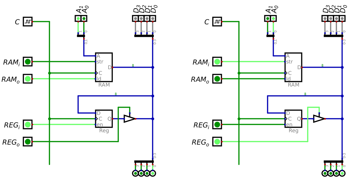
The left image shows the signals for moving the contents of memory address 01 to the register and the right
shows how to move the contents of the register to address 00. These two images correspond to the middle two
tows in the above table.
The left shows how to move the contents of address 10 to the register, and the right shows how to move the data
in the register to memory address 01. These two images correspond to the last two rows in the above table.
10.5. For Next Time
Check out the
Bus, RAM, and registerschematic for DigitalRead Chapter 2 Section 2 of your text
2 pages