8. Latches and Flip-Flops
The combinational logic topic covered circuits that did not store or require any stored data to operate
Here, circuits capable of storing data for later use will be covered
These can later be used to construct more complex circuits that make decisions based on a series of possible states
8.1. Set-Reset Latch (S-R Latch)
One of the most basic circuits for storing data is a set-reset latch (S-R latch)
What’s unusual about this circuit is that it has internal feedback
The output of the circuit is fed back into itself as input
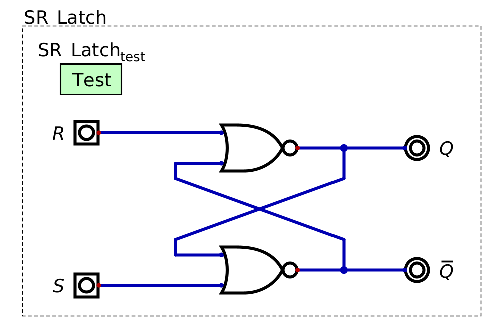
An S-R latch using NOR gates. The \(S\) means “set”, \(R\) is “reset”, \(Q\) is the bit being stored, and \(\lnot Q\) is the inverse of the bit being stored. Notice how the outputs of the circuit (\(Q\) and \(\lnot Q\)) also serve as two of the four inputs to the circuit.
Note
There are several possible designs for an S-R latch. The textbook uses a similar design to the above image, but uses two NANDs instead of NORs. Although this NAND based design would work slightly differently, the general idea is the same.
In an S-R Latch
\(S\) stands for “set” — set the stored bit to
1\(R\) stands for “reset” — clear the stored bit and set it to
0\(Q\) is the value of the bit being stored
\(\lnot Q\) is the inverse of the bit being stored
Since this circuit has internal feedback, it’s behaviour depends on the current state
The way it behaves when changing \(S\) or \(R\) depends on the current output
\(S\) |
\(R\) |
\(Q\) |
\(\lnot Q\) |
\(Q'\) |
\(\lnot Q'\) |
||
|---|---|---|---|---|---|---|---|
|
|
|
|
|
|
||
|
|
|
|
|
|
||
|
|
|
|
|
|
||
|
|
|
|
|
|
||
|
|
|
|
|
|
||
|
|
|
|
|
|
||
|
|
|
|
|
|
||
|
|
|
|
|
|
In the above table
\(Q/\lnot Q\) designate the state before changing \(S/R\)
\(Q'/\lnot Q'\) designate the state after changing \(S/R\)
Also note that \(Q/\lnot Q\) should never be equal
When \(S\) and \(R\) are both
0, the output state of the circuit will not changeThe values of \(Q\) and \(\lnot Q\), whatever they are, will not change
This is called the quiet state, or quiescent state
When \(S\) is set high, one of two things can happen
The circuit may be in a stable state, meaning the outputs do not change
This will happen when the output of \(Q\) is already
1
Alternatively, the circuit may be put into an unstable state, meaning the values of the output change
The outputs of this state are emphasized within the above truth table with
*This happens when the output of \(Q\) is
0This will cause \(Q\) to become
1This then causes the output of \(\lnot Q\) to also change, putting the circuit into a stable state
In practice, the unstable state will be resolved nearly instantaneously — on the order of nanoseconds
When \(R\) is set high, like with setting \(S\) high, one of two things can happen
The circuit may be in a stable state, meaning the outputs do not change
The circuit may be put into an unstable state, meaning the values change
The outputs of this state are emphasized within the above truth table with
**
Finally, if both \(S\) and \(R\) are high, the outputs are both
0, but this is an invalid stateIt’s not reasonable to set and reset at the same time
Further, having both \(Q\) and \(\lnot Q\) equal is inadmissible
One could do it, but there is no real utility in doing so
Activity
When the circuit turns on for the first time and all inputs are 0, what will the outputs of \(Q\) and
\(\lnot Q\) be?
8.2. Data Latch (D Latch)
The S-R latch can be modified to eliminate the ability for both set and reset to be high at the same time
Make it such that only one can be active at a time
This can be achieved by having a single input split into two signals
One of the two parts of the split signal is fed into the S-R latch
The other part is inverted before being fed into the S-R latch
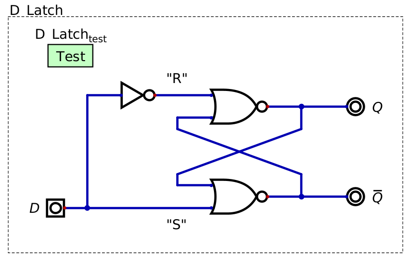
A D latch, which is a modified S-R latch. Here, \(D\) is the label for the input data. Like the S-R latch, \(Q\) is the bit being stored, and \(\lnot Q\) is the inverse of the bit being stored. The labels \(S\) and \(R\) are included here as a reference to what these inputs were called in the S-R latch, but are not typically included in diagrams of D latches.
The above figure shows how the S-R latch may be modified into what is called a Data latch (D latch)
The \(D\) means data
With this configuration, it’s not possible to have the \(S\) and \(R\) both be high at the same time
Or at least, the inputs that were \(S\) and \(R\) in the S-R latch
Unfortunately, however, it’s also not possible to have \(S\) and \(R\) both be low at the same time
This eliminates the quiet state, which was necessary for storing, or latching, the bit
When \(D\) is
1, \(Q\) is1When \(D\) is
0, \(Q\) is0
This D latch design effectively only relays the input to the output with no way to save data
8.2.1. D Latch with Enable
To store data, the D latch needs a way to enter the quiet state
Where \(S\) and \(R\) are
0
In other words, there needs to be a way to
Allow \(S\) and \(R\) to be
0at the same timeAllow \(S\) to be
1and \(R\) being0, and vice versaDisallow the ability for both \(S\) and \(R\) to be
1at the same time
This can be achieved with an enable input that can deactivate the NORs’ inputs
If the enable is off, \(S\) and \(R\) are both
0If the enable is on, relay the value’s of \(S\) and \(R\) to the NORs
By reintroducing the circuit’s ability to enter the quiet state, data can not be latched/stored
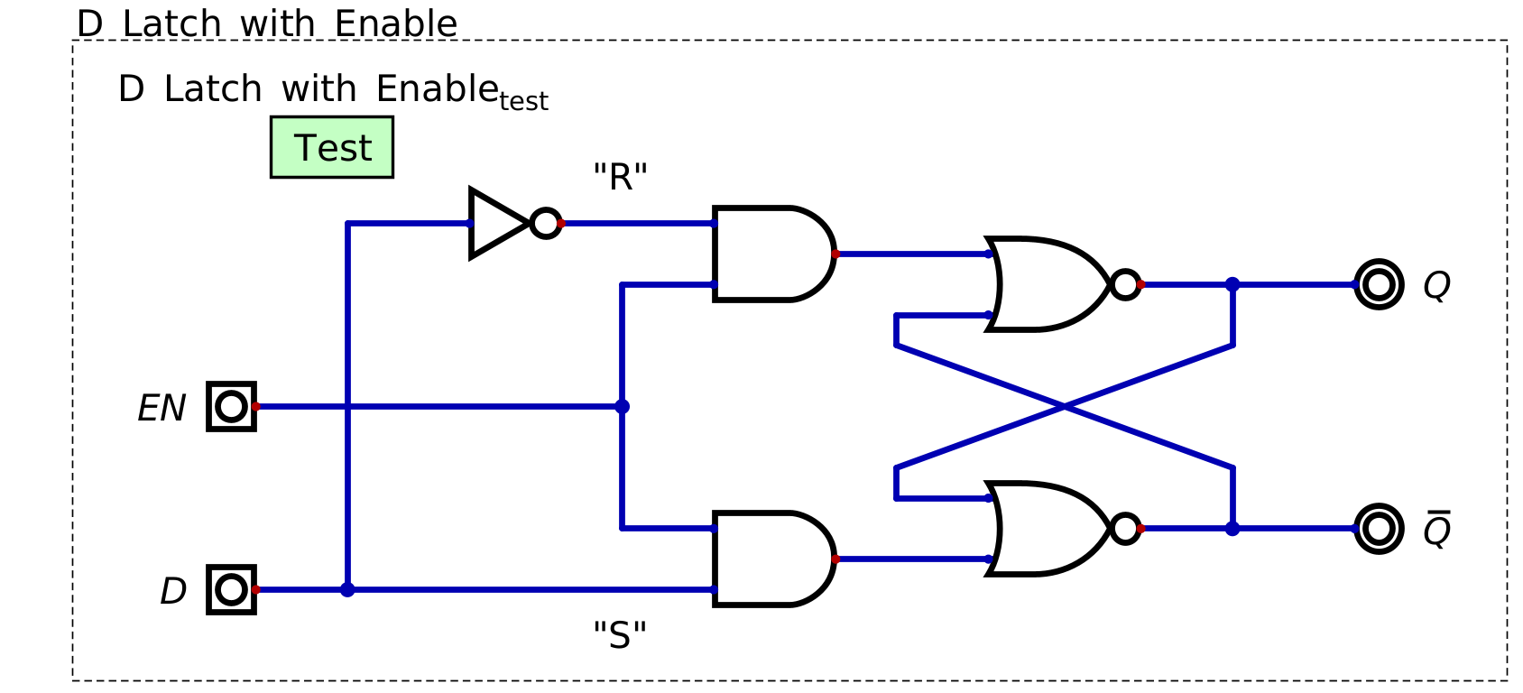
A D latch with an enable input. The enable input controls when the D latch is in the quiet state to store data (enable low) or when the data stored in the latch can be updated by toggling the \(D\) input (enable high). The labels \(S\) and \(R\) are included here as a reference to what these inputs were called in the S-R latch, but are not typically included in diagrams of D latches.
8.3. D Flip-Flop
A clock is a device within computers used to synchronize most of the components performing operations
It produces a periodic waveform at a constant frequency, jumping from low to high to low, etc.

Example clock signal. This signal has a constant frequency and oscillates between a low and high signal.
Typically, one would want to synchronize when data is stored in latches with the clock cycles
A simple solution to this is to use the clock signal as the enable signal for the D latch
However, the D latch with enable will change the value stored whenever the enable is high
For practical reasons, the data should only be latched the instant the clock pulses
One solution to this problem is to combine two D latches in series, but carefully control when each D latch is enabled
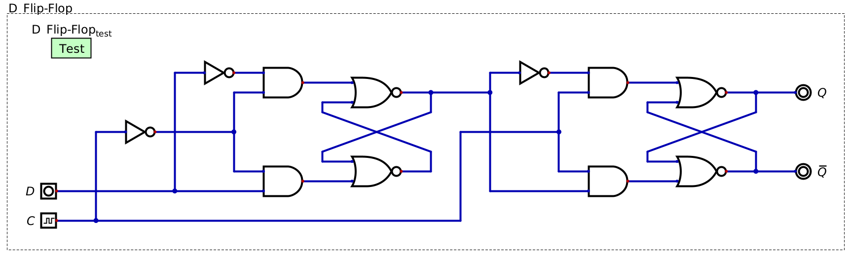
A D flip-flop made by combining two D latches. The enable is labelled \(C\) for clock and controls when each D latch is enabled. Notice how the clock’s enable line is inverted into the first D latch, meaning it’s not possible for both D latches to be active at once.
In the above figure, \(C\) is the label for the clock signal, which is serving as an enable for the D latches
Notice how the clock input is inverted before being fed into the first D latch, but not before the second D latch
Only one of the D latches can be in the quiet state at any time
When the clock signal is low
The first D latch is active and can store whatever is on the \(D\) input
The \(D\) input can toggle several times, which would change what the first D latch is outputting
However, the second D latch is in the quiet state, meaning that it’s output value does not change
In other words, the value of \(D\) does not affect the value of \(Q\)/\(\lnot Q\) at this stage
When the clock signal transitions to high
The first D latch enters the quiet state, meaning the last value of \(D\) is latched into the first D latch
The second D latch becomes active, latching in the value being output by the first D latch
At this time, \(D\) can change, but it will not impact the stored value as the first D latch is disabled
With this configuration, the value of \(D\) can never directly alter the value of \(Q\)/\(\lnot Q\)
The value of \(D\) must first move through the first D latch
8.3.1. D Flip-Flop Symbol
D flip-flops are a common tool used in digital circuits, and as such, are commonly represented with a single symbol
Below is an image of how D flip-flops are represented within Digital
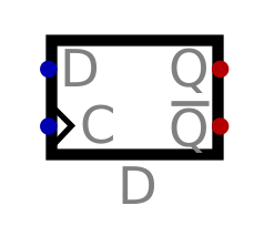
The symbol of a D flip-flop used within Digital. The triangle at the clock input is a common symbol used to denote a clock input.
8.4. For Next Time
Check out the
S-R Latchschematic for DigitalCheck out the
D Latch without Enableschematic for DigitalCheck out the
D Latch with Enableschematic for DigitalCheck out the
D Flip-Flopschematic for Digital