6. Combinational Logic
With an understanding of logic gates, more complex logic structures can be constructed
Here, structures that can make decisions based on some combination of inputs will be explored
6.1. Decoders
Consider a situation where an input signal controls two outputs, where only one should be active at a time
When the input signal is low, one of the two outputs is high
When the input signal is high, the other output should be high
Input |
Output a |
Output b |
|
|---|---|---|---|
|
|
|
|
|
|
|
Note
Until now, all truth tables were shown to demonstrate how the boolean operators worked, each taking some number of inputs and producing a single output. These truth tables were used to describe how each operator worked.
Here, the truth table is not describing any specific operator, but some desired functionality. The goal would then
be to construct some circuit with logic gates to produce the desired functionality. Further, it’s showing how the
desired functionality has more than one output. More specifically, when the input is 0, output a should be 0
and output b should be 1, and when the input is 1, output a should be 1 and output b should be 0.
Based on the truth table, how could this functionality be achieved with boolean operators?
Output a is the inversion of the input
Output b is simply the input
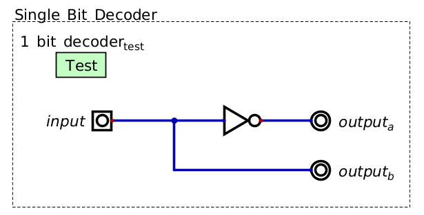
A single bit decoder. At any point in time, a single output is always high. The specific output that is high is controlled by the input signal.
This is an example of a single bit decoder
The one input signal can be thought of as a single bit
The input signal is “decoded” to control the output signals
6.1.1. More than One Input Bit
Now consider a situation where four separate circuits need to be controlled by a decoder
These circuits will be labeled 0 to 3 for ease
There needs to be a way to specify which of the four circuits should be running at any given time
Unfortunately, a single bit of information can only be decoded to two states —
0/1However, two input signals can have a total of four unique states
Continuing the idea that a signal can be thought of as a single bit, two signals can represent a two bit binary number
Each of these binary numbers could then correspond to each of the 0 – 3 circuits
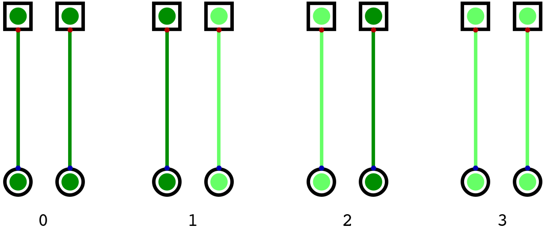
All four states two signals can represent. If treating the signals as bits, these correspond to the numbers, from left to right, \(00_{2}\), \(01_{2}\), \(10_{2}\), and \(11_{2}\), which correspond to the numbers \(0_{10}\), \(1_{10}\), \(2_{10}\), and \(3_{10}\) respectively.
The below truth table describes the desired functionality
Notice the relationship between the binary number the input signals represent and which output signal is high
Input a |
Input b |
Output 0 |
Output 1 |
Output 2 |
Output 3 |
|
|---|---|---|---|---|---|---|
|
|
|
|
|
|
|
|
|
|
|
|
|
|
|
|
|
|
|
|
|
|
|
|
|
|
|
To design a circuit for such functionality, think about each row and corresponding output at a time
Consider the first row and output 0
When input a is not high and input b is not high, output high for only output 0
This functionality can be achieved with a single two input AND with both inputs inverted
This gate will only output
1when both inputs are0Output 0 is \(\lnot a \land \lnot b\)
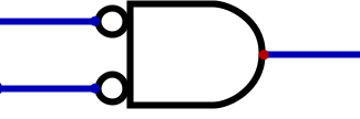
AND gate with two inverted inputs. This AND will only output 1 when both inputs are 0.
Now consider the second row and input 1
When input a is not high and input b is high, output high for only output 1
Output 1 is \(\lnot a \land b\)
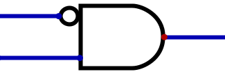
AND gate that will only output 1 when the input signal is 01, where the top signal is the most significant
bit.
Following this pattern, a two bit decoder can be a series of four AND gates with every combination of inverted inputs
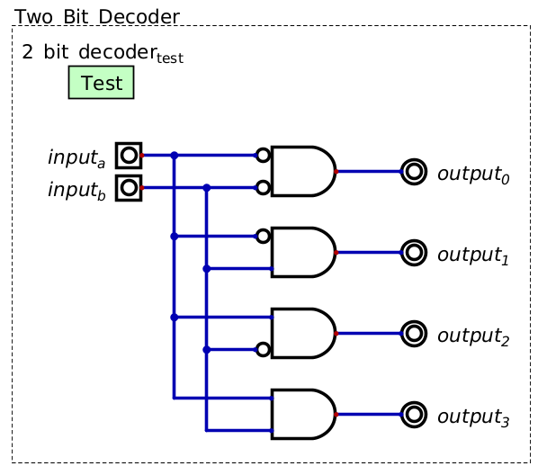
A two bit decoder, often called a 2-4 decoder. Two input signals are decoded to control a the four output signals. At any time, only one of the four output signals is high.
This particular design scales such that one can create decoders of any size
The only constraint, for lack of a better term, is the relationship between the number of inputs and outputs
Given \(n\) inputs, a total of \(2^{n}\) outputs can be controlled
In general, AND gates with various inverted inputs are ideal for situations where a specific input pattern is required
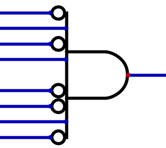
Example of an AND gate that only outputs 1 when an input pattern of 01010010, where the top input is the
most significant bit, is observed.
6.1.2. Decoder Symbol
Decoders are a common tool used in digital circuits, and as such, they are often represented with a single symbol
There is no universally set symbol for decoders, so the symbol used for decoders could differ
For this course, the symbol from Digital for decoders will be used

The trapezoid component represents a 2-4 decoder.
The above image shows a 2-4 decoder
Two inputs
Four outputs
Within this image, the input/output symbols are minimized for easier representation
Further, the two input signals are merged into a single signal line with a splitter/merger
One can think of the single line entering the decoder as two separate signals
The splitter/merger is used to simplify circuit designs to condense the number of signal lines
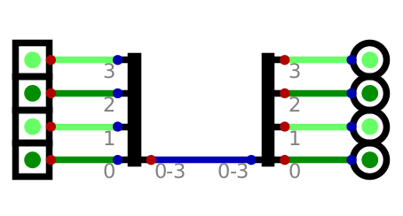
Example of four signals being merged into a single line and then being split into the four signal lines. This has no purpose other than to demonstrate how the splitter/merger works.
6.2. Multiplexers (Mux)
Multiplexers (mux) are used to select one of many input signal to to map to an output
The input signals could be arbitrary (high or low)
They only have a single output
In addition to input signals, multiplexers have selector signals to control which input is mapped to the output
The below truth table demonstrates the desired functionality for a 2 bit mux
Input a |
Input b |
Select |
Output |
||
|---|---|---|---|---|---|
|
|
|
|
||
|
|
|
|
||
|
|
|
|
||
|
|
|
|
||
|
|
|
|
||
|
|
|
|
||
|
|
|
|
||
|
|
|
|
Truth tables like this may be simplified such that the values of the input signals are treated as some variable
Input a |
Input b |
Select |
Output |
||
|---|---|---|---|---|---|
|
|
|
|
||
|
|
|
|
Here, the values of
XandYare not importantWhat is important is that the value
X/Yis mapped to the output based on the value of the select signalThis simplified view is not only smaller, but arguably makes the desired functionality more clear
Below is an image of a two bit multiplexer
The implementation idea is similar to that of a decoder in that it uses AND gates with inverted inputs
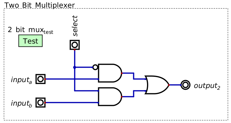
A two bit multiplexer. Two input signals are selected between with the selector. The value of the selected input signal will be mapped to the output.
One may notice that the input signals are never inverted on any gate, only the selector signal
This is because, if the gate for a given input is selected, the input should be directly mapped to the output
If the gate is selected and the input is
1, the AND gate outputs1If the gate is selected and the input is
0, the AND gate outputs0If the gate is not selected with the selector, the AND gate always outputs
0
Note
Notice that there is an OR gate before the final output signal. This OR’s only purpose is to combine all the outputs to a single line. However, one may wonder why it’s necessary to use an OR gate instead of simply combining the signals like in the below image.
Combining output signals on a single line directly creates problems and should not be done. This is true even if only one output line would be active at any given time. Instead, to combine output lines, use OR gates.
Connecting output signals like this will not work in practice. The nuanced reasoning for this is beyond the scope of
the course and depends on the configuration of the transistors and other components within the logic gates. But
briefly, often, when a gate outputs 0, its output is actually tied to ground. This means, if any other signal
connected to the line is 1, it will ultimately be pulled to ground through the gates outputting 0, thereby
making the whole line 0, even though it should be 1.
To avoid the problem, an OR gate is typically used to combine signals.
Below is a four bit multiplexer
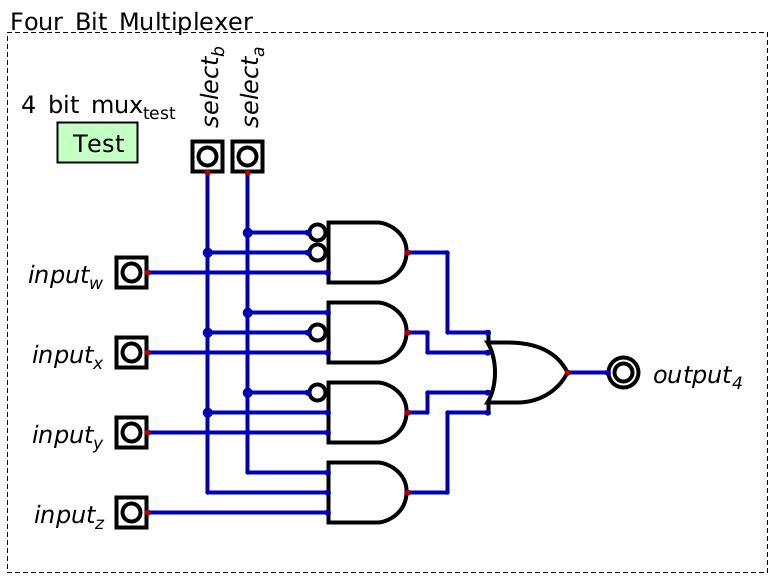
A Four bit multiplexer. This design will scale to any input size as long as there are sufficient selector lines.
Notice that the design is a scaled up version of the two bit multiplexer
This design scales such that one can create multiplexers of any size
Here, the constraint is that for \(2^{n}\) inputs, \(n\) selector bits are needed
6.2.1. Multiplexer Symbol
Like decoders, multiplexers are a common tool that are often represented with a single symbol
Unlike decoders, multiplexers have a common symbol, which is similar to the decoder’s symbol in Digital
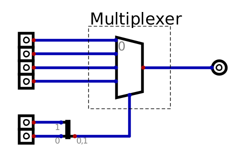
The trapezoid component represents a four bit decoder.
The above image shows a four bit multiplexer
Four inputs
Two selectors
One output
Within this image, the input/output symbols are minimized for easier representation
Further, the two select signals are merged into a single signal line with a splitter/merger
6.2.2. Demultiplexer (Demux)
A demultiplexer (demux) is another common tool
It is the inverse of a multiplexer
Take one input and output it to some selected output signal line

Multiplexer with an output directly connected to a demultiplexer.
Below is a simplified truth table with the functionality of a demultiplexer
Input |
Select b |
Select a |
Output 0 |
Output 1 |
Output 2 |
Output 3 |
||
|---|---|---|---|---|---|---|---|---|
|
|
|
|
|
|
|
||
|
|
|
|
|
|
|
||
|
|
|
|
|
|
|
||
|
|
|
|
|
|
|
One may notice that this is very similar to a decoder
The difference is that a demux maps an arbitrary value of the input to the output
A decoder always outputs
1
6.3. Programmable Logic Arrays (PLA)
Programmable logic arrays (PLA) are a general purpose design for implementing any boolean logic functionality
Can map any input to any desired output
PLAs are effectively decoders where the single decoded output signal may activate multiple final outputs
They consist of two main parts
A collection of AND gates, called an AND array, which acts as a decoder
A collection of OR gates, called an OR array, which activates an output when specific decoded signals are high
The number of AND gates depends on the number of inputs
Given \(n\) inputs, there will be a total of \(2^{n}\) AND gates
Like decoders
The number of OR gates depends on the number of desired output signals
One OR for each output
The number of inputs to each OR depends on the number of decoded signals that could activate the OR’s output
The OR gates serve as a way to connect multiple gate outputs to a single output
The idea of a PLA is best described with an example
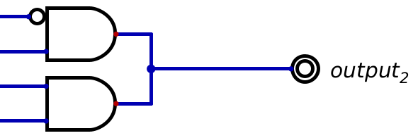
Below is a truth table describing some mapping of two input signals to three output signals
The outputs are arbitrary and have no meaning other than to provide some example
Input 1 |
Input 0 |
Output 0 |
Output 1 |
Output 2 |
|
|---|---|---|---|---|---|
|
|
|
|
|
|
|
|
|
|
|
|
|
|
|
|
|
|
|
|
|
|
|
To make the connection of input to output more clear, the truth table can be rewritten to include decoded inputs
In 1 |
In 0 |
D 0 |
D 1 |
D 2 |
D 3 |
Out 0 |
Out 1 |
Out 2 |
||
|---|---|---|---|---|---|---|---|---|---|---|
|
|
|
|
|
|
|
|
|
||
|
|
|
|
|
|
|
|
|
||
|
|
|
|
|
|
|
|
|
||
|
|
|
|
|
|
|
|
|
From the above table, when should each of the outputs be high?
Output 0 is high when the zeroth, second, or third decoded signals are high
Output 1 is high when the first or second decoded signals are high
Output 2 is high when the first, second, or third decoded signals are high
One may be tempted to map each decoded signal directly to the desired outputs, however, there are problems with this
As discussed above with the multiplexers
Instead, the decoded signals are mapped to OR gates that correspond to each output
The goal is then to
Create a decoder
Map the decoded signals to OR gates when the signal should cause the specific output to go high
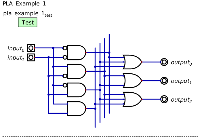
Programmable logic array (PLA) mapping two inputs to three outputs. The PLA is made up of an array of AND gates serving as a decoder and an array of OR gates that will output a high signal when any of the decoded inputs are high.
This basic design of an array of AND gates followed by an array of OR gates scales to arbitrary size
Below is some truth table describing some functionality for a three input, four output PLA
Input c |
Input b |
Input a |
Output a |
Output b |
Output c |
Output d |
|
|---|---|---|---|---|---|---|---|
|
|
|
|
|
|
|
|
|
|
|
|
|
|
|
|
|
|
|
|
|
|
|
|
|
|
|
|
|
|
|
|
|
|
|
|
|
|
|
|
|
|
|
|
|
|
|
|
|
|
|
|
|
|
|
|
|
|
|
|
|
|
|
The PLA matching the functionality described in the above truth table is shown in the following image
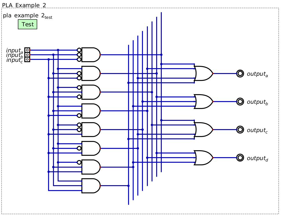
Programmable logic array (PLA) mapping three inputs to four outputs. This figure shows how the general design of an array of AND gates followed by an array of OR gates can be scaled up.
6.3.1. Programmable Logic Array/Look Up Table Symbol
One may have realised that this functionality is effectively a dictionary/map/look up table
In fact, within Digital, PLAs are called look up tables
Below is a figure of a look up table from Digital
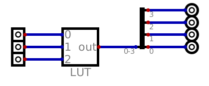
Example of a look up table from Digital. This specific look up table maps three inputs to four outputs.
Note
Look up tables are an abstract idea, and as such, the physical implementation is often not important. In practice, these look up tables could be PLAs, constructed with arrays of AND gates and OR gates, or they could be implemented with a form of memory mapping the input to some memory addresses, which in turn contains the desired output within that memory location.
6.4. Functional Completeness
As seen with PLAs, any boolean logic function can be implemented systematically
In other words, any function can be physically created with configurations of AND, OR, and NOT gates
This means that the set of {AND, OR, NOT} gates is Functionally complete
Although other gates exist, they are not necessary for implementing any function
Nevertheless, they may make configuring a circuit for some functionality simpler
However, review De Morgan’s Laws
\(\lnot a \lor \lnot b = \lnot (a \land b)\)
\(\lnot a \land \lnot b = \lnot (a \lor b)\)
This shows that, with OR and NOT gates, one can create the functionality of an AND gate
\(\lnot(\lnot a \lor \lnot b) = \lnot(\lnot (a \land b)) = a \land b\)
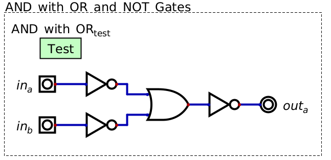
Implementation of and gate functionality with only or gate and not gates.
Similarly, with AND and NOT gates, the functionality of an OR gate can be created
\(\lnot(\lnot a \land \lnot b) = \lnot(\lnot (a \lor b)) = a \lor b\)
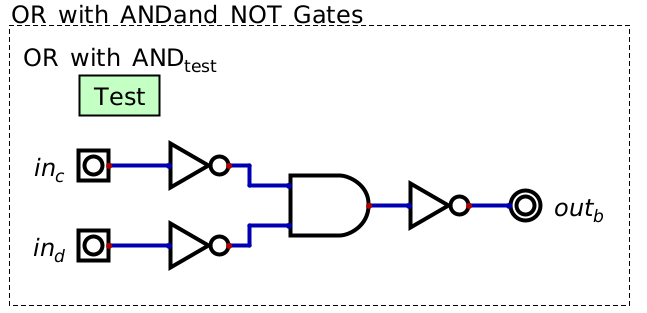
Implementation of and gate functionality with only or gate and not gates.
Therefore, the set of {AND, NOT} and {OR, NOT} are also functionally complete
6.4.1. Minimal Set
One may wonder if a single gate type is sufficient to have a functionally complete set
To prove this is the case, all one needs to do is show that the single gate type can
Implement the \(not\) operation
Implement the \(and\) operation
Implement the \(or\) operation
Seeing the reduced sets made up of {AND, NOT}/{OR, NOT}, one may wonder if {NAND} and {NOR} are functionally complete
Activity
Show that {NAND} and {NOR} are functionally complete.
6.5. For Next Time
Check out the
Decoderschematic for DigitalCheck out the
Multiplexerschematic for DigitalCheck out the
Programmable Logic Arrayschematic for DigitalCheck out the
Functional Completenessschematic for DigitalRead Chapter 3 Sections 5 of your text
3 pages