18. Instructions and Microcodes
Although RAM has currently only held data, computation has been performed on the system
With careful manipulation of the control signals, specific operations were executed by the system
Reading and writing to RAM
Performing arithmetic
Outputting values
Looping
Realizing this, it becomes possible to create a set of well defined instructions for the system
18.1. Constraints
The designers of the computer (us) decide what instructions to include and how they are to be performed
However, it is important to consider the limitations and constraints of the system
Although the ESAP system is to be fully functional computer, it is limited by the fact that it’s an 8 bit system
RAM is byte addressable
The main bus is 8 bits wide
Thus, the information on the bus can only be 8 bits
This information includes data
But also includes instructions
Details on what the instructions are and how the system deals with them will be covered later
For now, consider that, for the ESAP system, individual instructions for the system will be made up of two parts
Operator (specifying an operation)
Operand
For example, imagine an instruction to load data from a RAM address into register A
The operator is — load data into register A
The operand is — the RAM address of the data to be loaded into register A
This means, there needs to be a way to encode the operator and the operand into the 8 bits
There needs to be a way to encode load into A and the memory address of the data to load into A
A design decision must be made here — how many bits for each of the two parts?
For the ESAP system, the most significant 4 bits will be for the operator, and the remaining 4 will be for the operand
This means, a total of 16 unique operators and 16 unique operands can be represented
If the operand is a memory address, with 16 unique values, only 16 memory address may be indexed
This is why the system was designed with only 16 bytes or RAM

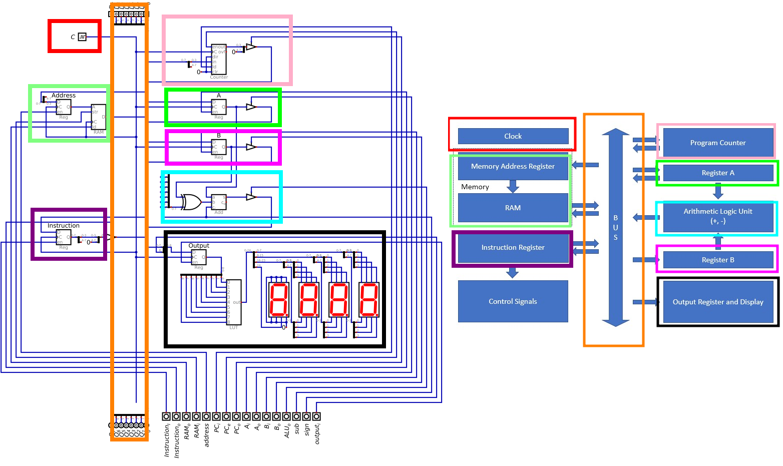
The ESAP system’s 8 bit instruction broken down into the two parts — operator and operand. The 4 most significant
bits, represented as XXXX would specify some operator, while the 4 least significant bits, represented as
YYYY would be the operand.
Ultimately, it is possible to have different breakdowns of the 8 bits
For example, 3 and 5 could have been used for the operator and operands respectively
3 bits for the operator — 8 total
5 bits for the operand — 32 total
But there is always going to be a trade off
Less vs. more flexibility with the number of operators, at the cost/benefit of operands and address space
As previously mentioned, more details are to come on how the system encodes and manages the instructions
For now, the takeaway is understanding how the 8 bits constrains the system’s instructions
18.2. Microcodes
In several previous topics, it was observed that instructions were performed by moving data around the system
Moving data around to different modules
Some modules output data, while others input
Consider the instruction of loading data from some memory address into register A
Any of the 16 memory addresses could be used in this example, but
15(0b1111) is used here
Think about the steps involved to perform this instruction within the context of the ESAP system design
Load the value of the target memory address (
0b1111) from the bus into the memory address registerOutput the value stored in RAM to the bus and input the value from the bus into register A
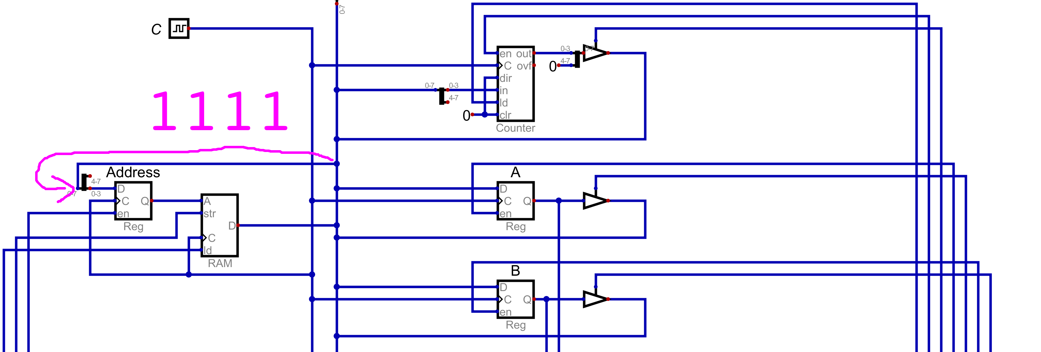
Subsection of the ESAP system so far, corresponds to step 1 above. From the bus, load into the memory address
register the address of the data to be accessed from RAM. Here, the address is 15, or 0b1111.
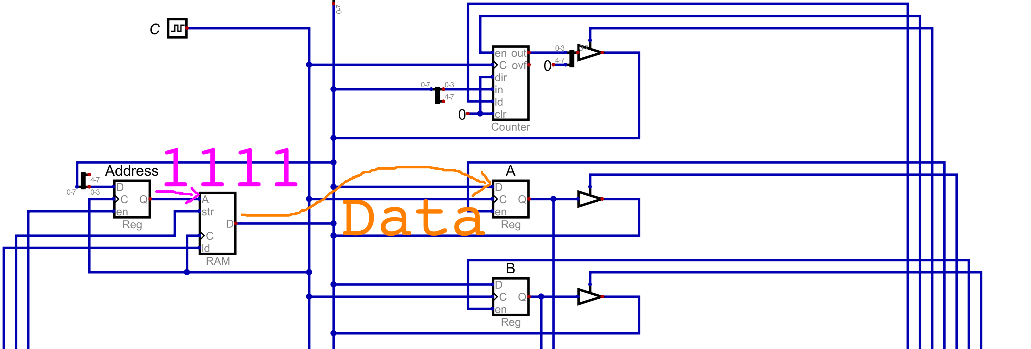
Subsection of the ESAP system so far, corresponds to step 2 above. Output the data stored in RAM address 15
(0b1111) to the bus, and input the data from the bus into register A.
Below is a table showing how the control lines would be configured for the two steps
Like before, due to space limitations, the clock column has been removed and several columns have been combined
\(Address\) |
\(RAM\) |
\(A\) |
\(B\) |
\(ALU\) |
\(out\) |
\(PC\) |
|---|---|---|---|---|---|---|
|
|
|
|
|
|
|
|
|
|
|
|
|
|
These two steps put together achieve the instruction of loading data from a specific RAM address into register A
The individual steps are called microcodes
Each of these microcodes took one clock cycle
Most instructions are made up of several microcodes
These instructions would be things like loading data from RAM, addition, outputting data, etc.
Additional instructions are to be discussed shortly
Thus, individual instructions may take multiple clock cycles
18.3. Fetch and Instruction Register
Remember, RAM stores both instructions and data
Continuing the above example of loading data from RAM to register A
Although the control logic to perform this action was discussed above, the instruction must have first come from RAM
The instruction would need to be fetched from RAM
Instructions will be stored sequentially within RAM, starting at address 0
The program counter starts at 0, and keeps track of the address of the next instruction to be executed
Thus, to get the next instruction from RAM, the value from the program counter must be sent to the address register
Then, it can be output from RAM to the bus
However, as previously discussed, the data on the bus is transient
The bus needs to be free to transmit data around the system while performing the instruction
The instruction must be stored somewhere for processing
Therefore, a new register will be created — the instruction register
This instruction register will store the instruction for the duration of its execution on the system
Thus, the instruction from RAM must be moved to the instruction register
And finally, the program counter needs to be incremented
Update it to store the value of the next instruction to be executed
\(Address\) |
\(RAM\) |
\(A\) |
\(B\) |
\(ALU\) |
\(out\) |
\(PC\) |
\(Instruction\) |
|---|---|---|---|---|---|---|---|
|
|
|
|
|
|
|
|
|
|
|
|
|
|
|
|
The above table shows the control logic configuration for the fetch cycle
Note that, incrementing the program counter does not require the data bus
It is isolated from moving data from RAM to the instruction register, and can therefore happen at the same time
Ultimately, this fetch cycle is the first part of any instruction
All instructions must be fetched from RAM and put into the instruction register for processing
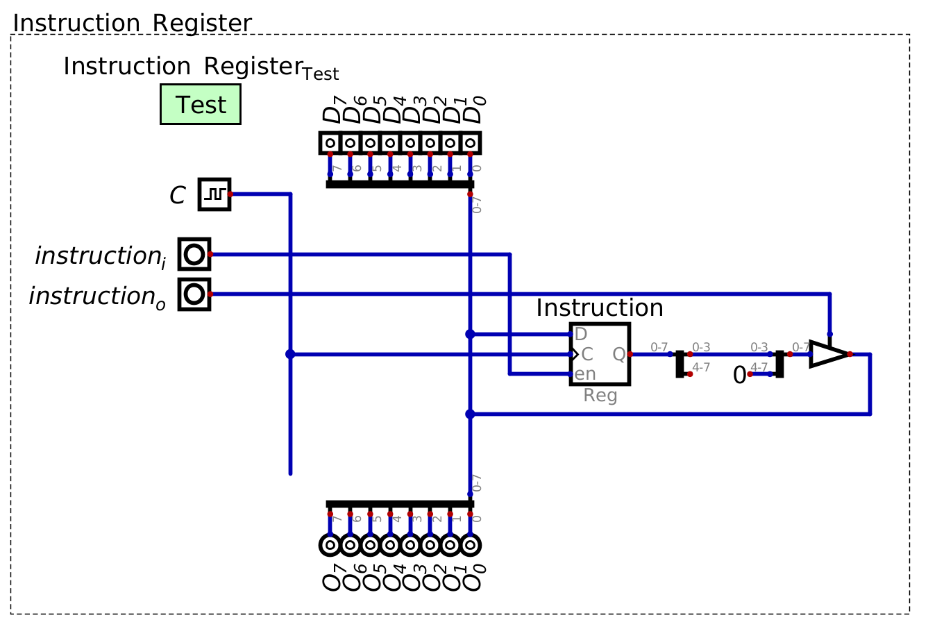
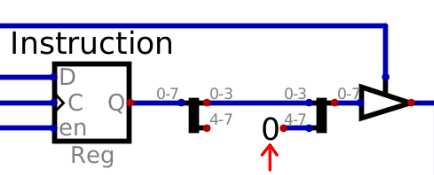
Configuration of the instruction register. Only the least significant four bits of the register can output to the bus as this would be the four operand bits from the instruction. The four most significant bits, corresponding to the operand of the instruction, is yet to be used.
Above is a configuration of the instruction register
Consider the example in the previous section of loading data from RAM into register A
The 8 bit instruction is
XXXX YYYYThe four bits
XXXXis some bit pattern designating the operand for loading data from RAM to register AWhat the pattern for the operand is at this stage is not important
The four bits
YYYYis the operand, specifying some RAM addressThe value of
YYYYis variableThe above example used
0b1111, or15
The least significant four bits must be loaded into the address register to specify the address to load data from
In other words, the value of these lower four bits must be able to be put back onto the main bus
This allows the system to move the variable data operand between the different modules for manipulation
The value of the most significant four bits,
XXXX, can remain in the instruction register for processing
Configuration of the ESAP system with the ALU, RAM, output, program counter, and instruction register modules connected.
The below tables shows the control logic for all steps required to load data from RAM to register A
The first two rows correspond to the fetch cycle
The second two corresponds to loading data from RAM to register A
This table is almost a concatenation of the two previous tables
The only difference is that the control logic for the instruction register is present for both parts
The fetch part and the loading data from RAM to register A
It was not present in the first table showing the control logic for loading data from RAM to register A
\(Address\) |
\(RAM\) |
\(A\) |
\(B\) |
\(ALU\) |
\(out\) |
\(PC\) |
\(Instruction\) |
|---|---|---|---|---|---|---|---|
|
|
|
|
|
|
|
|
|
|
|
|
|
|
|
|
|
|
|
|
|
|
|
|
|
|
|
|
|
|
|
|
Comparison of the current system with the instruction register and the ESAP architecture overview.
18.4. Instruction Set
The instruction set is a collection of instructions the computer can execute on the hardware
Like the example instruction discussed, loading data from RAM into register A
Consider the functionality that would be required for a typical computing system
Move data round the system
Perform arithmatic operations
Output data
Loop
Conditions/make decisions
As discussed, with 4 bit operators, a total of 16 unique instructions can be implemented for the ESAP system
Each of the 16 instructions can be uniquely identified with a bit pattern
The specific instructions included in the instruction set is up to the designers of the system (us)
The designers get to decide which instructions the computational system can perform
Assuming the hardware is sufficient to perform such an instruction
Below are 13 instructions that can be included on the current system
This leaves room for additional instructions to be added to the instruction set later
These 13 were chosen to balance a few considerations
Small number of instructions while still providing a breadth of functionality
Minimizes the amount of RAM required to describe a whole program
Minimizes the number of clock cycles/microcodes the instructions take
Further, the 13 instructions that are included may be changed at a later time by the designers
One may discover that certain instructions are redundant or entirely unnecessary
Refining the instruction set may allow for more, different and useful instructions to be included
The process of refining the instruction set is a form of optimization for computational systems
How each instruction’s bit pattern ultimately manages the control logic of the system will be discussed later
Here, only the instructions, along with their bit pattern, are presented
For the ESAP system, the instruction’s bit pattern is somewhat arbitrary
What matters is that each bit pattern uniquely identifies an instruction
18.4.1. The 13 Instructions
Below is a table summarizing the instruction set
Following the table is a description of each instruction
Bit Pattern |
Hex |
Label |
Description |
|---|---|---|---|
|
|
|
No Operation |
|
|
|
Load A From RAM |
|
|
|
Load A Direct |
|
|
|
Load B From RAM |
|
|
|
Load B Direct |
|
|
|
Save A to RAM |
|
|
|
Save B to RAM |
|
|
|
Add B to A — |
|
|
|
Subtract B from A — |
|
|
|
Jump Always |
|
|
|
No Operation |
|
|
|
No Operation |
|
|
|
No Operation |
|
|
|
Output Unsigned Integer |
|
|
|
Output Signed Integer |
|
|
|
Halt |
0000—NOOPNo Operation
An instruction that takes a known number of clock cycles, but ultimately means do nothing
This may seem silly, but there are practical reasons for this operation
For the ESAP system, this operation can be used as a time delay
0001—LDARLoad data into register A from some specified RAM address
The 4 bit operand for this instruction specifies some memory address to read the data from
Consider the full 8 bit instruction
0001 YYYY0001, the operator, specifies theLDARinstructionYYYY, the operand, would be the memory address to read the data from
The high level microcode steps would be as follows
Output the operand (memory address) from the instruction register and put it into the address register
Output the value from RAM and put it into register A
0010—LDADLoad the provided data directly into register A
The 4 bit operand for this instruction is the data to be loaded into RAM
Can only load 4 bit data into RAM through this instruction
Reduces the amount of RAM needed for loading data into register A when working with small numbers
Consider that
LDARrequires 2 memory addressesOne for the instruction
Another for the memory address of the data to be loaded into A
The high level microcode steps would be as follows
Output the operand (data) from the instruction register and put it into register A
Warning
This load direct instruction has a limitation caused by the underlying hardware — only positive integers can be loaded directly to the register.
Since each operand is only 4 bits wide, but the data bus is expecting 8 bits, the 4 most significant bits are padded with zeros.
Consider the 8 bit number
0b11111111. Although this number may be255or-1, depending on if it is a signed integer, adding0b00000001to this number results in0b1_00000000regardless. This number is256, but because only 8 bits can be represented and the overflow carry bit is ignored, the number is ultimately truncated to0.However, consider the 4 bit number
0b1111, which may be15or-1. The programmer may intend for this bit pattern to mean-1, but the operand for the load direct instructions are only four bits wide and are padded with zeros, thus this bit pattern would become0b00001111when it is added to the register. This 8 bit number, signed or not, is15and adding1to this number results in0b00010000.One may try to address this issue with hardware and additional logic, but one must ask — is this additional complexity worth it?
0011—LDBRLoad data into register B from some specified RAM address
Similar to
LDAR
0100—LDBDLoad the provided data directly into register B
Similar to
LDAD
0101—SAVASave the data from register A to some specified RAM address
The 4 bit operand for this instruction specifies some memory address to write the data to
The high level microcode steps would be as follows
Output the operand (memory address) from the instruction register and put it into the address register
Output the value from the A register and put it into RAM
0110—SAVBSave the data from register B to some specified RAM address
Similar to
SAVA
0111—ADABAdd the contents of register B to register A —
A += BThis overwrites the contents of register A
This instruction has no operand
The high level microcode steps would be as follows
Output sum from the ALU and put it into register A
1000—SUABSubtract the contents of register B from register A —
A -= BThis overwrites the contents of register A
This instruction has no operand
The high level microcode steps would be as follows
Set the subtraction signal high and output difference from the ALU and put it into register A
1001—JMPAJump to the instruction at the specified memory address
This sets the program counter to the specified address such that it stores the next instruction to be run
The 4 bit operand for this instruction specifies the memory address to jump to
The address of the instruction to run next
The high level microcode steps would be as follows
Output the operand (address to jump to) from the instruction register and put it into the program counter
1010,1011, and1100—NOOPNo Operation
Same as
0000aboveLeft open for potential additional instructions
1101—OUTUOutput data as an unsigned integer from some specified RAM address
The 4 bit operand for this instruction specifies some memory address of the data to be output
The high level microcode steps would be as follows
Output the operand (memory address) from the instruction register and put it into the address register
Output the value from RAM and put it into the output register
1110—OUTSOutput data as a signed integer from some specified RAM address
Similar to
OUTUThe high level microcode steps would be as follows
Output the operand (memory address) from the instruction register and put it into the address register
Set the sign signal high and output the value from RAM and put it into the output register
1111—HALTStop the program
This will effectively deactivate the clock
The high level microcode steps would be as follows
Send some control signal to turn deactivate the clock
Activity
Consider the ESAP system’s current hardware.
What other instructions could be included?
What variations of the existing instructions could be included?
18.5. For Next Time
Something?