14. Address Register and RAM
RAM stores data and instructions for the computer
The values in RAM are temporary
RAM is not designed for long term storage
It is designed to store values the computer is working with
Although RAM was discussed in earlier topics, it is time to incorporate it into the ESAP system design
14.1. RAM Module
As previously discussed, memory stores data in individually indexable memory locations called addresses
The number of unique memory addresses is called the address space
Each location stores some amount of data, called the addressability
The amount of data in a memory location is independent from the number of memory addresses
Most computers are byte addressable, meaning each memory location stores one byte of data
This is not a requirement, however
The total amount of data storable is the size of the address space times the addressability
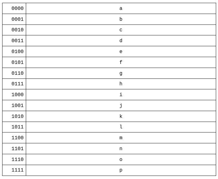
Visualization of RAM. The left column is memory addresses, and the right is the data stored at the respective memory address.
In the above example, a total of 16 unique memory addresses exist
Each address is represented as a row in the table
The memory address is included in the left column of the table
This means, in this example, there is an address space of 16
Locations
0b0000–0b1111Or,
0x0–0xF
With an address space of 16, a total of four bits would be required to index each memory address
The data stored in each of the 16 memory address is represented as the 16 letters
The letters
a–p, one in each rowIn the image, the addressability is not represented; one cannot determine the amount of data in each location
In the current ESAP system being built, the address bus and data bus are partially shared
However, even though the data bus has a total of 8 bits, only 4 bits will be used to index memory
The reasons for this is due to how program instructions will be encoded
4 bits for the instruction and 4 for an operand
Details on how instructions are encoded will be covered in detail in a later topic
Thus, the reasons for this limitation will be made clear later
With 4 bits, a total of 16 unique memory locations can be indexed
The system will store 1 byte in each memory location, like most systems
A total of 8 bits will be stored in each memory location
This means the system can store up to 16 bytes of data in RAM
Note
Until the late 2000s/early 2010s, a typical computer used a 32 bit address space. One of the limitations of such a system is that 32 bits could index \(2^{32}\), or \(4,294,967,296\) unique memory addresses. This may feel like a lot, but to put this into perspective, that’s only \(4GB\).
14.1.1. Address Register
Having the memory addresses and data share a bus poses a problem for the system
The values on the bus are always changing, but the indexed memory location may need to be static for some time
A not particularly useful configuration of a RAM component with a shared address and data bus.
Consider the above configuration of RAM in a system with a shard address and data bus
Mind the splitter used
Remember, only 4 bits are used to index memory
Thus, only the 4 least significant bits are useful for indexing RAM
The 4 most significant bits are ignored
Is it possible, for example, to store the value 4 in memory address 2?
It’s possible to index memory address 2 by configuring the data on the bus to
0b00000010But as soon as the value 4 is added to the bus (
0b00000100), memory address 4 is indexed, not 2
The problem is, the memory address indexed in RAM will always be based on what value is currently on the bus
Therefore, there needs to be a way to isolate the memory address from the value on the data bus
A simple solution to this problem is to add an address register
Input the memory address to index into the address register
This value will be unchanged until explicitly updated
The address value stored in the address register will be what is indexing RAM
Now the data on the bus can change without impacting the memory address being indexed
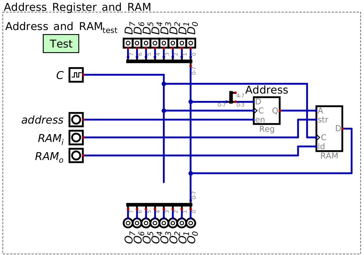
A configuration of RAM component with an address register facilitating the separation of a memory address and the changing values stored on the bus.
With this configuration, there is now a small, but isolated address bus
The line connecting the output of the address register and the RAM component’s address input
Between the register’s \(Q\) and RAM’s \(A\)
To return to the previous example problem, it is now possible to load the value 4 into memory address 2
Configure the data on the bus to be 2 (
0b00000010)Load the value from the bus into the address register with the \(address\) control signal
Configure the data on the bus to be 4 (
0b00000100)Load the value from the bus into RAM with the \(RAM_{i}\) control signal
14.2. Including RAM in the System
To include the RAM module, connect the corresponding components up to the existing ESAP ALU system
Each of the control signal lines are moved to the bottom of the system
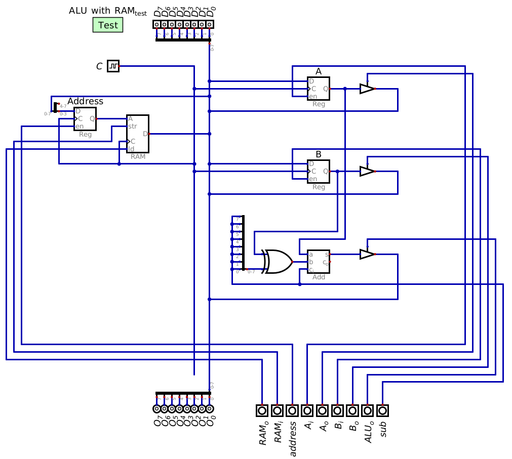
Configuration of the ESAP ALU with RAM added to the system.
Notice that the RAM module was added to the left hand side of the data bus
This is a design/style decision; it is not important that it is placed here
Motivation for putting it on the left is
It will correspond to the ESAP system architecture overview already discussed
The image would get too long/tall if every component/module was stacked on the right hand side of the bus
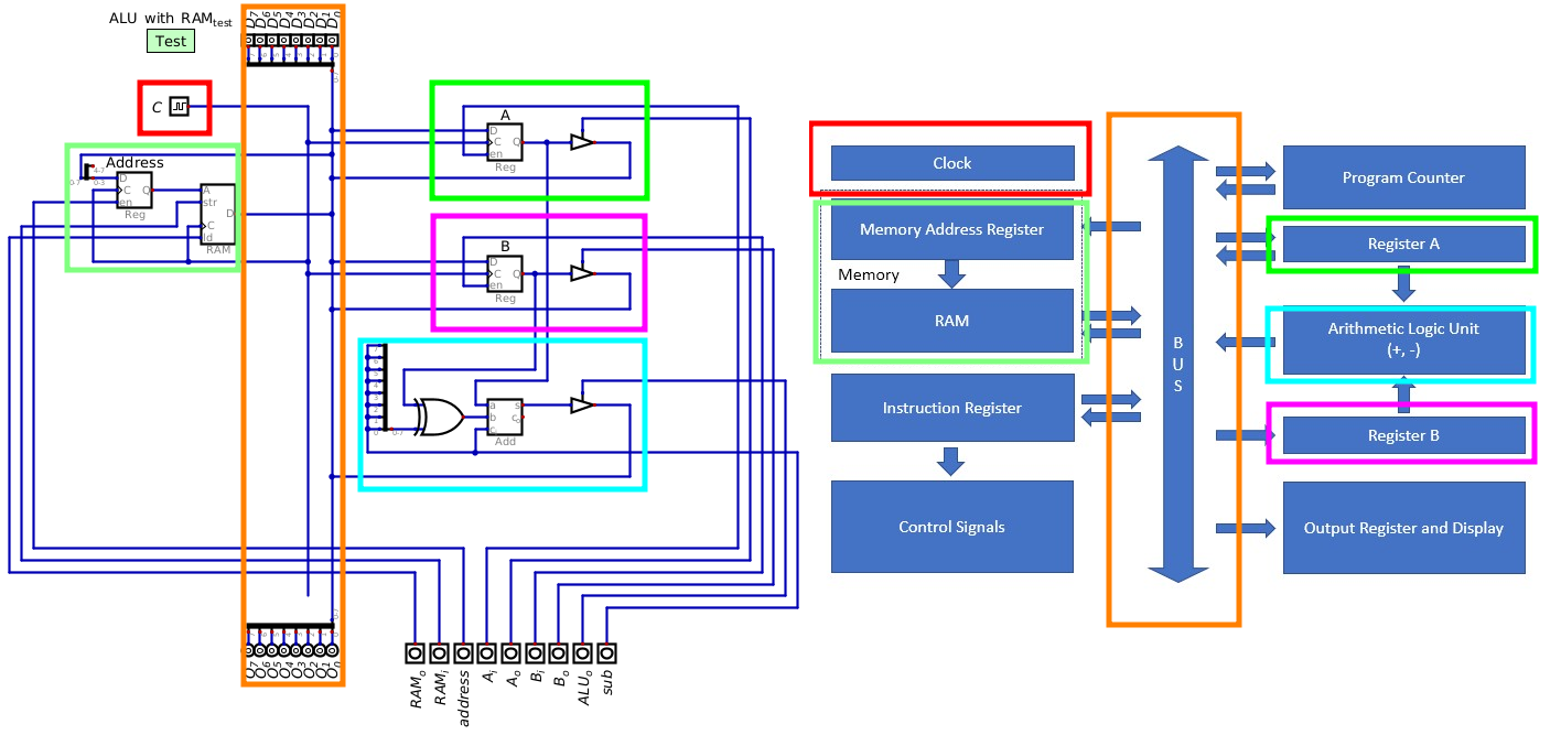
Comparison of the ALU with RAM and the ESAP architecture overview.
14.2.1. Executing Arithmetic on the ALU with RAM
Like in the previous topic, consider performing arithmetic on arbitrary numbers
This time, the numbers will be loaded to RAM, which will later be accessed to perform the operations
For an example, consider calculating \(15 + 4 - 7\)
For demonstration purposes, the high-level program to be executed on the system will be as follows
Load the data into RAM
Calculate the sum of 15 and 4 and save the result to RAM
Calculate the difference between the calculated sum and 7 and save the result to RAM
Like in previous topics, the below tables represent programs
However, due to space limitations, if a module has an input and output control signal, their columns are combined
Values will be represented as
input/outputFor example, a low input, but high output would be represented as
0/1
\(Address\) |
\(RAM\) |
\(A\) |
\(B\) |
\(ALU_{o}\) |
\(sub\) |
\(D\) |
\(C\) |
||
|---|---|---|---|---|---|---|---|---|---|
|
|
|
|
|
|
|
|
||
|
|
|
|
|
|
|
|
||
|
|
|
|
|
|
|
|
||
|
|
|
|
|
|
|
|
||
|
|
|
|
|
|
|
|
||
|
|
|
|
|
|
|
|
With the data loaded into RAM, the next steps are to load the data from RAM, perform addition, and save the result
\(Address\) |
\(RAM\) |
\(A\) |
\(B\) |
\(ALU_{o}\) |
\(sub\) |
\(D\) |
\(C\) |
||
|---|---|---|---|---|---|---|---|---|---|
|
|
|
|
|
|
|
|
||
|
|
|
|
|
|
|
|
||
|
|
|
|
|
|
|
|
||
|
|
|
|
|
|
|
|
||
|
|
|
|
|
|
|
|
||
|
|
|
|
|
|
|
|
Since the goal is to now subtract 7 from the result, it would be fine to save the result back into register A
But for demonstration purposes, the result is being saved to RAM first
The next step is to load more data from RAM to perform subtraction and save the result
\(Address\) |
\(RAM\) |
\(A\) |
\(B\) |
\(ALU_{o}\) |
\(sub\) |
\(D\) |
\(C\) |
||
|---|---|---|---|---|---|---|---|---|---|
|
|
|
|
|
|
|
|
||
|
|
|
|
|
|
|
|
||
|
|
|
|
|
|
|
|
||
|
|
|
|
|
|
|
|
||
|
|
|
|
|
|
|
|
||
|
|
|
|
|
|
|
|
If everything worked correctly, the contents of RAM should be
Address 0 — 15
Address 1 — 4
Address 2 — 7
Address 3 — 19
Address 4 — 12
14.3. For Next Time
Something?