13. Arithmetic Logic Unit and the ESAP
The Arithmetic Logic Unit (ALU) is a combinational logic circuit for integer arithmetic and logical operations
ALU designs can vary significantly and has implications for the total design of the computer
13.1. The Idea of the ALU
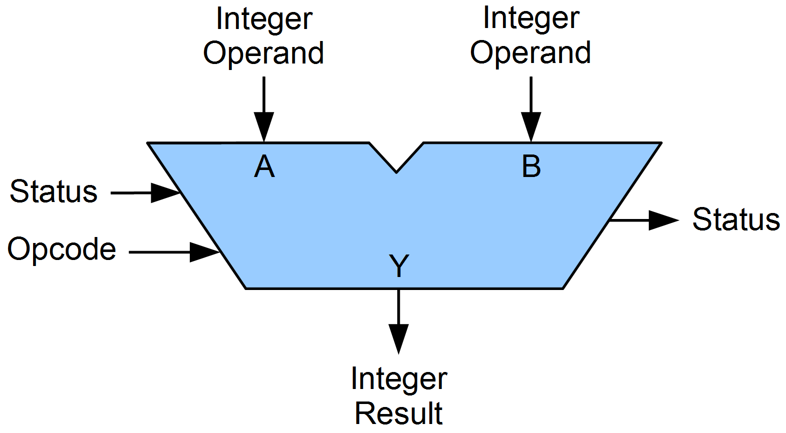
Generic symbol for an ALU.
With sophisticated ALUs, some operation is applied to the inputs (operands) to produce some output
The operator is specified with some opcode passed to the ALU
These operations may include
Addition/Subtraction
Increment/Decrement
AND/OR/XOR/NOT
Bit Shift/Rotate
Further, the ALU may update the system’s status flags, and, in turn, may behave differently depending on the flags
For example, the system may remember if the last operation resulted in an output of zero
Status flags are a topic to be discussed later
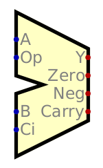
Digital does not have a built in ALU like the other components discussed so far
However, it does have a custom ALU one can import
Although, this custom ALU will not be used here
Digital’s importable ALU.
Designing a sophisticated ALU is not difficult
However, integrating one into a larger architecture may challenging
Thus, to start, a simple ALU will be built and used
Even with the simple ALU, the system being designed will be Turing Complete
Note
One may have noticed that the ALU is effectively a function that takes inputs to produce outputs. However, one may also notice that this function may have side effects — changing system status flags.
In your computer science courses there has been a strong emphasis on avoiding side effects and writing pure functions, which this seems to violate. For better or worse, under the hood, the common modern designs/architectures for computers are very stateful and full of side effects.
Fortunately, as one goes to higher levels of abstraction, like software, systems are designed such that side effects can be eliminated, despite the fact that the underlying hardware is stateful.
13.2. The Eater Simple as Possible Architecture (ESAP)
The base architecture for the system being built is the Simple as Possible (SAP) design [1]
Created by Malvino & Brown
For this course, a modified version of the SAP architecture by Ben Eater is used
This architecture will be referred to as Eater’s SAP, or ESAP
Ben Eater has a YouTube playlist of him physically building this computer on breadboards
Note, however, that slight modifications to this design are made for the purposes of this course
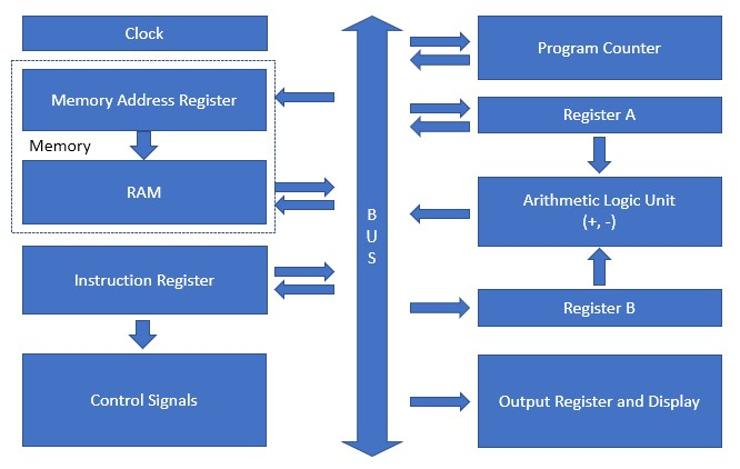
Overview of the ESAP Architecture. Arrows show how data is transferred between components of the computer system. With this design, the address and data bus are not entirely separate. This overview does not show the control bus.
The design is simple to follow and understand, while still being Turing Complete
Further, it is straightforward to add to
It will also serve as the basis of going deeper in architecture complexity
The ALU will serve as the starting point for building a computer with this architecture
13.3. Design of the ESAP ALU
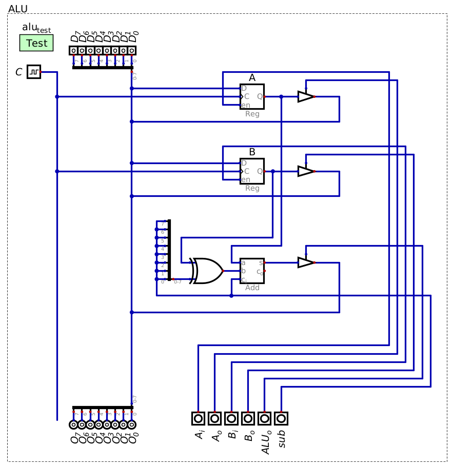
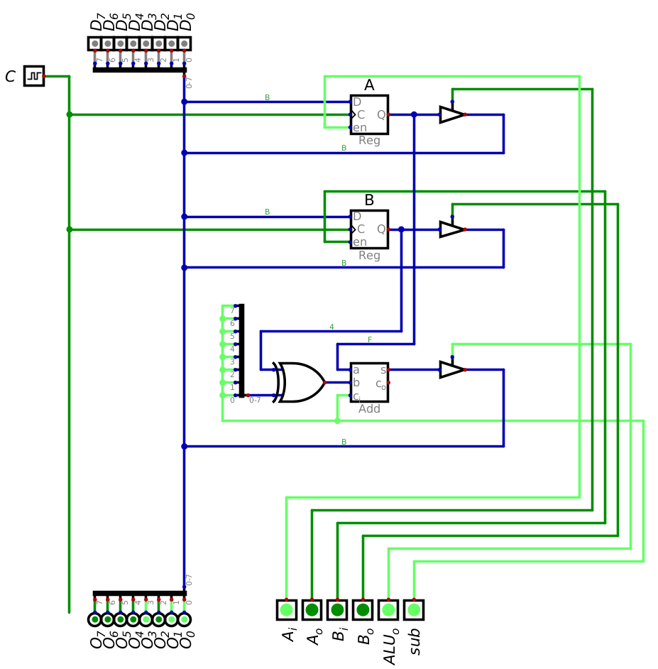
Configuration of the ESAP ALU connected to a data bus and control bus within Digital. This ALU always calculates the sum (or difference) of the integer values stored in registers A and B.
The ESAP ALU is only capable of performing addition and subtraction
A control line (\(sub\)) controls if the ALU performs addition or subtraction
The ALU is always calculating the sum/difference of the two integer values stored in registers A and B
Loading from the data bus into the registers is controlled by \(A_{i}\) and \(B_{i}\)
There is control logic for the registers to output to the data bus (\(A_{o}\) and \(B_{o}\))
There is no control for the registers’ output to the adder
Thus, the adder always has the sum/difference of whatever data is stored in A and B
Although the ALU is always calculating the sum/difference, its output is controlled with a control signal
\(ALU_{o}\)
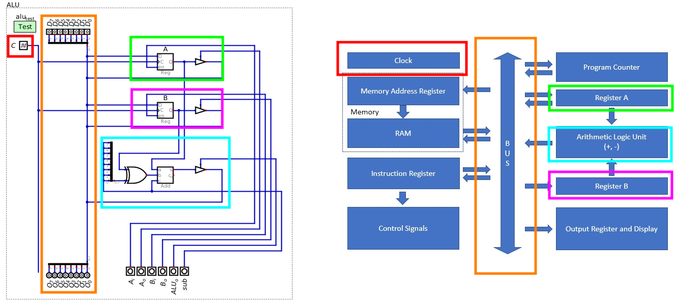
Comparison of the ALU and the ESAP architecture overview. This ALU includes several parts of the whole ESAP design — two registers, ALU, clock, and data bus. The ALU does include the start of the control bus for the whole system (the vertical signal lines on the right hand side of the ALU), which is not shown in the architecture overview.
It is possible to see how the ALU fits into the whole ESAP architecture design
With the ALU, several components of the whole system are present
Register A
Register B
ALU
Data bus
Clock
Further, the ALU does include the start of the control bus for the system
This is not shown in the ESAP architecture overview
A control bus will be required for the system to function
One may have noticed the layout of register B and the ALU are swapped
ALU is below both registers in the Digital design, but between the registers in the overview
This difference is effectively irrelevant
As long as the inputs/outputs are configured correctly, this will have no functional impact on the system
However, there is one slight difference that will have a functional impact on the system — register B out
The designed ALU’s register B can receive input from and output to the data bus
But the architecture overview shows that register B can only receive input
Adding the ability to output from register B does provide some additional, yet minimal, flexibility to the design
The original design does not allow for outputting from register B due to physical constraints and the minimal benefit
Remember, the original design was physically built on breadboards
13.4. Executing Arithmetic on the ESAP ALU
With careful control over which parts of the system are inputting and outputting, a program can be run on the ALU
In the same way data was swapped between RAM and registers in an earlier topic
As an example, consider the problem of adding the numbers 15 and 4 together
Based on the configuration of the ALU, think about the individual steps that would need to be performed
Load the number 15 into register A
Load the number 4 into register B
Output the sum from the ALU to the data bus
Note
For brevity, hexadecimal will be used to encode binary numbers where appropriate. Fortunately, it is simple to convert numbers between bases when they are powers of each other, as previously discussed here.
Consider that \(2^{4} = 16\). It is possible to take groupings of 4 bits and easily convert it a single hexadecimal digit. Further, it is possible to take an 8 bit binary number and convert it to two hexadecimal digits.
Given some 8 bit binary number —
0b01101011Split the number into two groups of 4 bits —
0b0110and0b1011Convert the 4 bit numbers into their hex digits —
0x6and0xBPut the digits together to form the two digit hex number —
0x6B
This patten would also work with more groupings of four bits.
Note that 0b and 0x prefixed the binary and hexadecimal numbers to eliminate ambiguity. These are common
prefixes used in computing.
Below is a table showing how to add the numbers 15 and 4 together with the ALU
Like with the bus, this is not so much a truth table, but a program
Cmeans clock pulseZis a high impedance state
\(A_{i}\) |
\(A_{o}\) |
\(B_{i}\) |
\(B_{o}\) |
\(ALU_{o}\) |
\(sub\) |
\(D\) |
\(C\) |
||
|---|---|---|---|---|---|---|---|---|---|
|
|
|
|
|
|
|
|
||
|
|
|
|
|
|
|
|
||
|
|
|
|
|
|
|
|
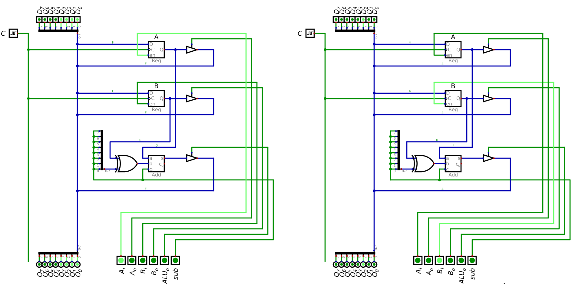
The left image shows the signals to load the value 15 (0x0F) into register A, and the right shows the signals to
load the value 4 (0x04) into register B. A clock pulse would be required in both scenarios to have the data
latch into the registers. These images correspond to the first two rows in the above table.
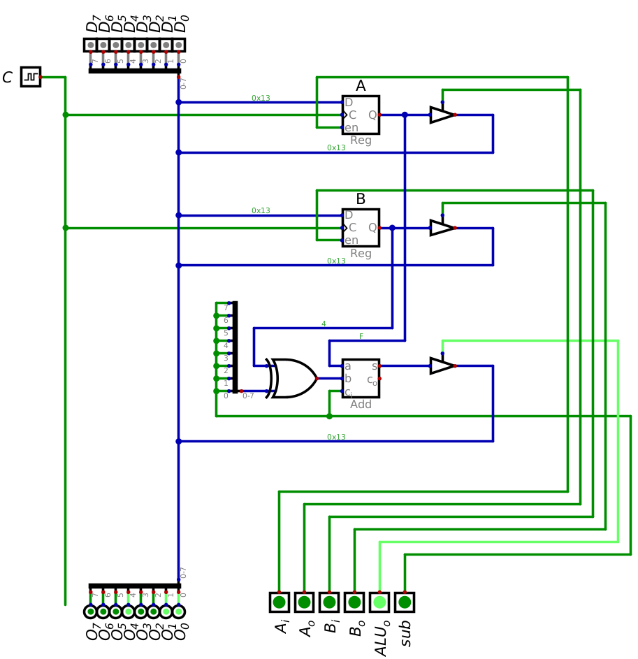
Signals to output the sum of registers A and B to the data bus. This image corresponds to the third and final row in the above table.
There is no need for a final clock pulse to output from the ALU
After executing the program, the result of the addition is output to the data bus
15 + 4 = 19
0b00001111+0b00000100=0b000100110x0F+0x04=0x13
To provide another example, consider the problem of 15 - 4, but storing the result into register A
Load 15 into register A
Load 4 into register B
Set the subtraction control signal
Output from the ALU
Store the result into register A
Output from register A
Below is a table representing the above program
Notice how, in this example, several steps are able to be performed in a single clock pulse
Namely, setting subtraction, outputting from the ALU, and inputting into A
\(A_{i}\) |
\(A_{o}\) |
\(B_{i}\) |
\(B_{o}\) |
\(ALU_{o}\) |
\(sub\) |
\(D\) |
\(C\) |
||
|---|---|---|---|---|---|---|---|---|---|
|
|
|
|
|
|
|
|
||
|
|
|
|
|
|
|
|
||
|
|
|
|
|
|
|
|
||
|
|
|
|
|
|
|
|
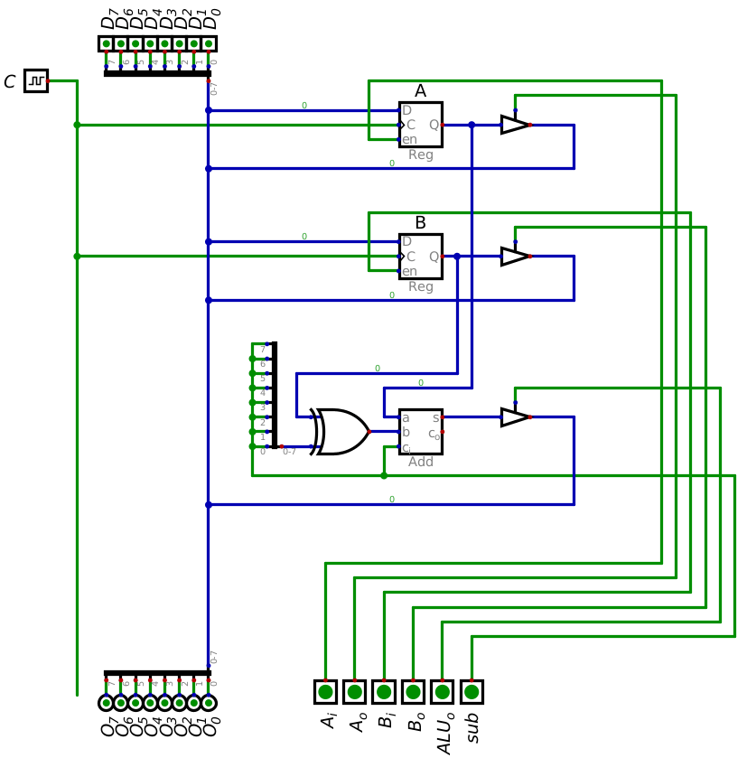
After executing the program, the result of the subtraction is stored in A and output to the data bus
15 - 4 = 11
0b00001111-0b00000100=0b000010110x0F-0x04=0x0B
Below is an animation of the program being executed
Animation of (a) loading 15 into register A, (b) loading 4 into register B, (c) outputting and saving the difference to register A, and (d) outputting the contents of register A to the data bus.
Note
Be mindful of the current state of the system. Consider what is happening when outputting the difference from the ALU to register A before and after the clock pulses.
State of the system before the clock pulse to output the difference of A and B back into A.
In the above image showing the state of the system before the clock pulse, it is clear that the output of the system
is 11 (0b00001011).

State of the system immediately following the clock pulse to output the difference of A and B back into A.
However, after the clock pulse, the output changes to 7 (0b00000111), which is not the correct difference. In
fact, it appears to have applied the operation twice (15 - 4 - 4 = 7).
Nevertheless, based on the state of the system, everything is correct. Remember, when the clock pulsed, the difference was stored into register A, the ALU is always calculating the sub/difference of the contents of the registers, and the ALU is still outputting to the data bus as per the control signal. In other words, the value on the data bus will in fact be the result of applying the operation twice. However, the true result of the subtraction is safely stored in register A.
13.5. For Next Time
Something?