9. Registers and RAM
D flip-flops allow one to store a single bit of information
However, they always update what’s stored on every clock pulse
In many cases, one wants more control over when the stored data in the D flip-flop is updated
9.1. Registers
D flip-flops have several uses, but they always update the stored value every time the clock pulses
If the data line is low, then the D flip-flop will store a
0on a clock pulseIf the data line is high, then a
1is stored on a clock pulse
However, for general purpose memory, the goal is to leave the stored data alone for several clock cycles
In other words, there needs to be a way to toggle when the signal on the data line is to be stored on a clock pulse
When enabled, store the data on the data line when the clock pulses
When not enabled, ignore the data on the data line and leave the stored data unchanged when the clock pulses
One way this can be achieved is to still update the stored value on every clock pulse
However, it will update to either
The value on the data line
The value that is already stored
This means there will effectively be two data lines
The actual data line
A feedback line from the D flip-flop’s output
Then, all that is needed is a multiplexer to toggle between which of the two data lines should be read form

A D flip-flop with enable, which can be used as a register. When the \(EN\) signal is low, the multiplexer selects the \(Q\) signal, meaning the value of \(Q\) will be fed back into the D flip-flop, which will be re-latched on a clock pulse, leaving the value stored effectively unchanged. When \(EN\) is high, the value from the \(D\) line will be latched on a clock pulse.
This type of structure is called a D flip-flop with enable, and can be used as a register
For registers, it is common to ignore \(\lnot Q\)
The two data lines are
\(D\) — the actual data line
\(Q\) — the output of the D flip-flop
The multiplexer in front of the D flip-flop allows for selecting which data line’s signal is stored
When \(EN\) is low
The multiplexer selects the \(Q\) line
The value of \(D\) is ignored
The value of \(Q\), whatever it is, will be re-latched into the D flip-flop on a clock pulse
The value stored in the register is effectively unchanged
When \(EN\) is high
The multiplexer selects the \(D\) line
The value of \(Q\) is ignored
The value of \(D\), whatever it is, is latched into the D flip-flop on a clock pulse
The value stored in the register is updated
Note
One may wonder, why go through the trouble of using a multiplexer and feeding the output \(Q\) back into the circuit when one could simply AND the clock signal with the enable signal? If this were the case, when \(EN\) is low, no clock pulse will reach the D flip-flop, when \(EN\) is high, clock pulses can pass through the AND gate. In other words, this simpler design would function perfectly as a D flip-flop with enable.
One could absolutely do this; however, in practice, although this can work, it would cause a slight delay in the clock signal which could cause problems. Usually, it’s a good idea to leave the clock signal alone.
9.1.1. Storing More than a Bit
A D flip-flop with enable can act as a register to effectively store a single bit of information
To store more than a single bit, configure multiple registers in parallel
For example, to store 8 bits/1 byte of data, stack eight registers together
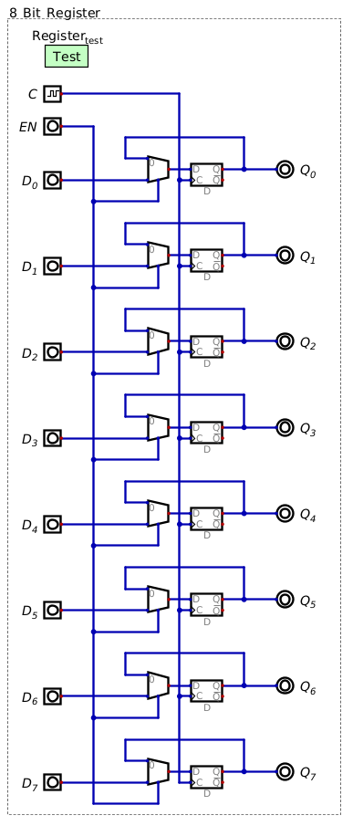
Eight D flip-flops with enables (registers) configured in parallel such that they can store eight bits/one byte of information. A single \(EN\) signal controls when all bits are stored in the register.
The design shown above can scale such that an arbitrary number of bits can be stored
9.1.2. Register Symbol
Many components are represented as a box
For example, D flip-flops and registers are both represented as boxes
However, these components are differentiated by their input labels and sometimes a label
In Digital, registers are represented with the following symbol
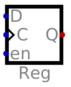
The symbol of a register within Digital.
In the above figure, notice how the \(\lnot Q\) output is not included
Typically, for registers, this output is not included
If one truly needs it, invert the \(Q\) output
Digital also allows the user to edit a register component to store a specified number of bits
If more than one bit is to be stored, the data lines would need to be combined with a merger component
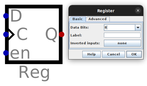
A register component within Digital capable of storing 8 bits of data.
9.2. Random Access Memory
Without knowing how to actually store data, the high level idea of RAM was previously discussed
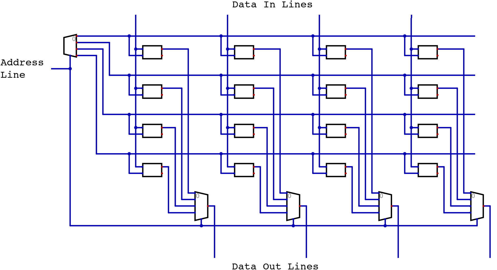
Visualization of an incomplete 4x4 block of RAM.
To review, above is a 4x4 block of RAM
There are four 4 bit memory addresses
A decoder is used to select which memory address is active
Notice how the decoded line activates all bits within a memory address
Multiplexers are used to relay the stored data out from the selected memory address
Notice that there is a multiplexer for each of the 4 bits in the memory addresses
Since registers (D flip-flops with enable) can be used to store data, they can be used for building RAM
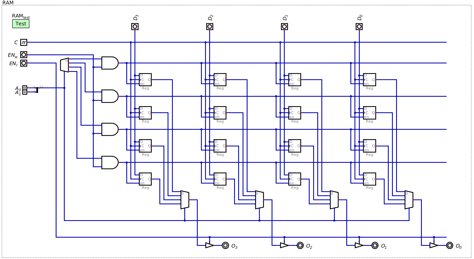
A 4x4 block of RAM using registers to store bits with controllable inputs, a clock signal, and read/write enables.
The above figure is a modified version of the same idea
Here, 1 bit registers are used to store the data
A clock signal is included
Controllable inputs for the memory address are added
Controllable inputs for the input data along with outputs are included
This design also includes a control over when data is written to RAM
Additionally, it includes a control over when data is read from RAM
9.2.1. Controlling Writes
When using a decoder to select a memory address, one of the decoded signals is always going to be high
This creates a problem as one of the memory addresses would be written to every clock pulse, even if not intended
Thus, there needs to be a way to have more control over when data is written to a memory address
One possible way to address this problem is to have a write enable signal toggle if clock pulses reach the registers
This can work, but as discussed above, it may create problems in practice
In general, it is best to not manipulate the clock signal
An alternative is to have a write enable signal control if the decoded signals are active or not
This can be achieved by ANDing an enable signal with each decoded signal
Below is a figure showing the relevant portion of the 4x4 block of RAM
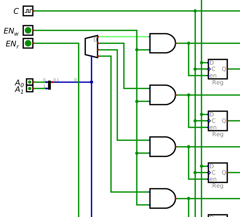
Controlling writes with a write enable signal. Here, the memory address selected is 00, which means the
corresponding decoded signal (top) after the decoder is active. However, since \(EN_{w}\) is low, the decoded
signal can not reach the registers at memory address 00.
9.2.2. Controlling Reads
Similar to the decoder, multiplexers will always be outputting the selected signal
However, it is desirable to have control over when a signal is being read/output from RAM
Here, a problem arises
Typically, several computer components share a collection of signal lines to transfer data
This shared collection of signal lines is called the bus
The bus will be discussed in more detail in the subsequent topic
Therefore, it is important that only specific components are reading/writing form the bus at a time
Otherwise, the signals on the bus could become corrupted and lose meaning
The trouble here is, when a component is outputting a low signal, it isn’t simply outputting nothing
Instead, the component connects the signal line to ground, thereby sinking the signal
Trying to put any data on a signal line that is sunk to ground would result in it also being sunk to ground
In other words, there needs to be a way to output a
0, a1, and to output nothingThis is where a driver comes in
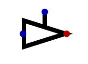
A driver component capable of allowing a signal to pass only when the control signal is high. When enabled, the input signal is relayed to the output. When enable is low, the driver’s output signal is in a high impedance state, meaning there is effectively no output.
A driver is a component that can act as a switch
When the driver is active, it relays, or drives, the input signal to the output
When it is not active, it is in a “high impedance”, or “high-Z” state
This effectively means the driver outputs nothing
This facilitates tri-state logic
01Z(nothing)
Therefore, drivers are an ideal tool for controlling when RAM is being read from
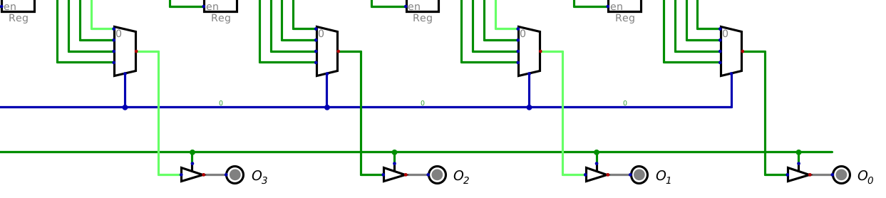
Drivers controlling when data is being read from RAM. Here, despite the data being read from RAM being 1010, as
seen by the multiplexer signal lines, the \(EN_{r}\) signal is low, meaning the drivers are in a high impedance
state, thereby effectively outputting nothing.
9.2.3. RAM Symbols
Digital provides several variations of RAM, most of which will not likely be used in this course
Two that are likely to be used will be
RAM with separate data ports
RAM with a shared data port
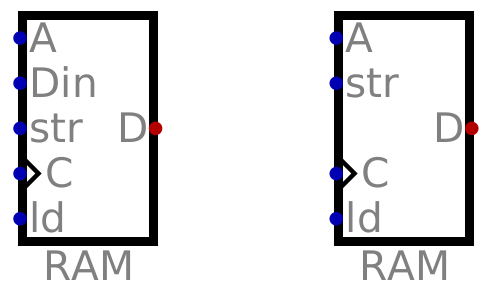
Two examples of RAM symbols. The left symbol represents RAM with two separate data ports — data can only be written to RAM through the \(D_{in}\) input, and data can only be read from the \(D\) output. The right symbol represents RAM with shared data ports — both reads and writes happen from the same \(D\) input/output.
The RAM with separate data ports has
Independent input and output lines
Data can only be written to RAM through the \(D_{in}\) input line
Data can only be read from RAM through the \(D\) output line
The RAM with a shared data port has
Shared input and output lines
Data is written to and read from RAM through the single \(D\) line
The RAM design discussed above aligns with the RAM with separate data ports
However, it can be modified to share the same data line by connecting the outputs back to the input lines
Note
The style of RAM discussed here is called static RAM (SRAM), and is a very high quality, but expensive way of making RAM. Whatever data is latched into RAM will remain there until power is removed from the circuit.
In modern computers, a different style called dynamic RAM (DRAM) is often used. The nuanced details of which will not be covered here, but briefly, instead of using a form of latch to store a bit, DRAM uses a single transistor and a capacitor, which stores a temporary charge that needs to be continuously re-charged by a separate circuit.
9.3. For Next Time
Check out the
1 bit registerschematic for DigitalCheck out the
1 byte registerschematic for DigitalCheck out the
RAMschematic for DigitalRead Chapter 3 Section 6 of your text
14 pages