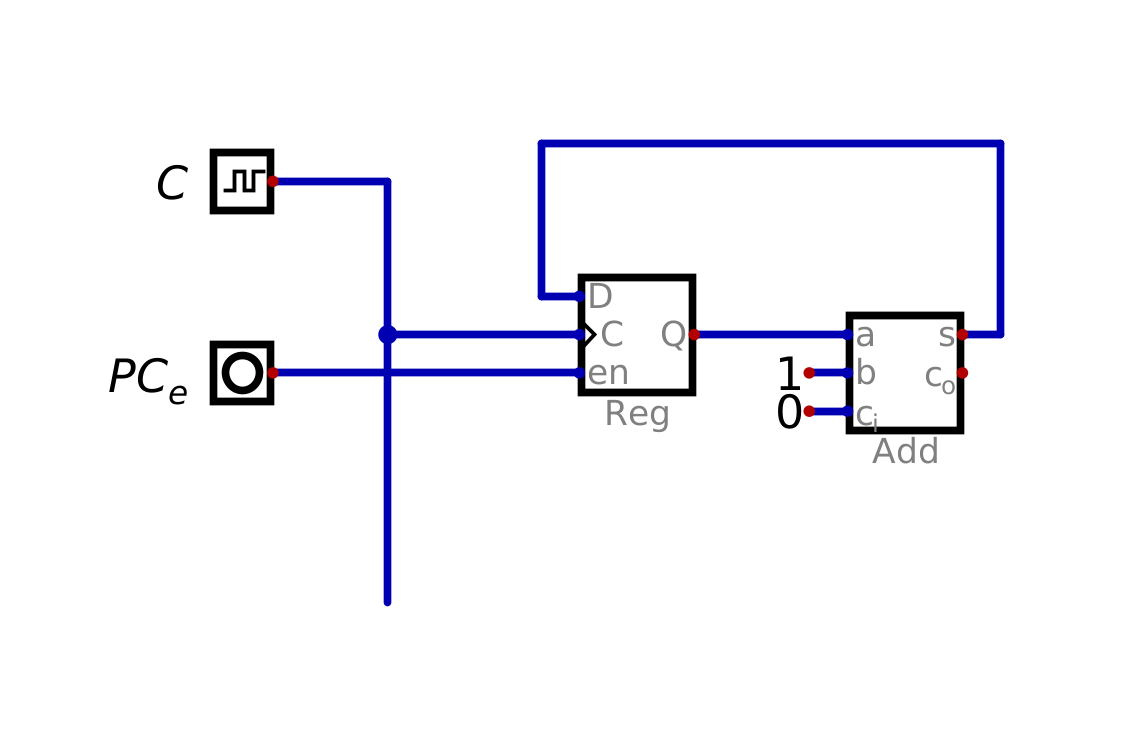
Configuration of a register and adder set to add 1 to the value in the register. Although the adder is always adding
one to the value stored in the register, the value in the register only updates when the \(PC_{e}\) signal is
high.
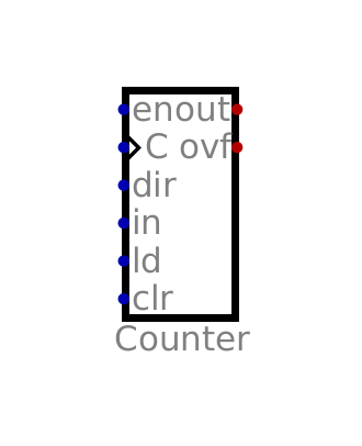
Storing a value can be achieved with a register
Incrementing a value can be achieved with an adder set to only ever add 1 to some inputted value
With the above configuration, the adder is always adding 1 to the value stored/output by the register (\(Q\))
The adder’s carry in is set to 0 and the carry out is ignored
However, even though the value at the register’s \(D\) input is always \(Q+1\), it only updates when enabled
When the \(PC_{e}\) control signal is set high
This design provides control over when the counter increments
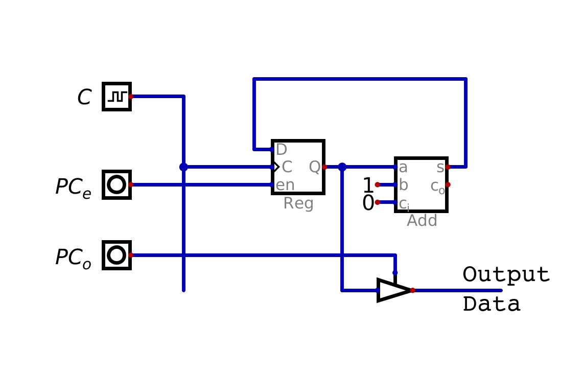
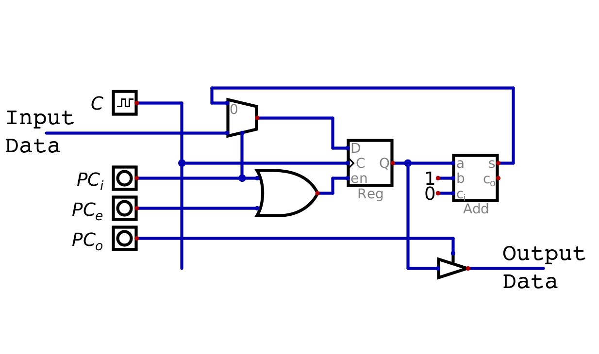
A driver can be used to control when the counter’s value is output. Note that the counter’s output is the register’s
output (\(Q\)), not the output of the adder (\(S\)).
To control the output, use a driver like in previous designs
Note, the counter’s output is \(Q\) — the register’s output
The output of the adder is for updating the state of the counter
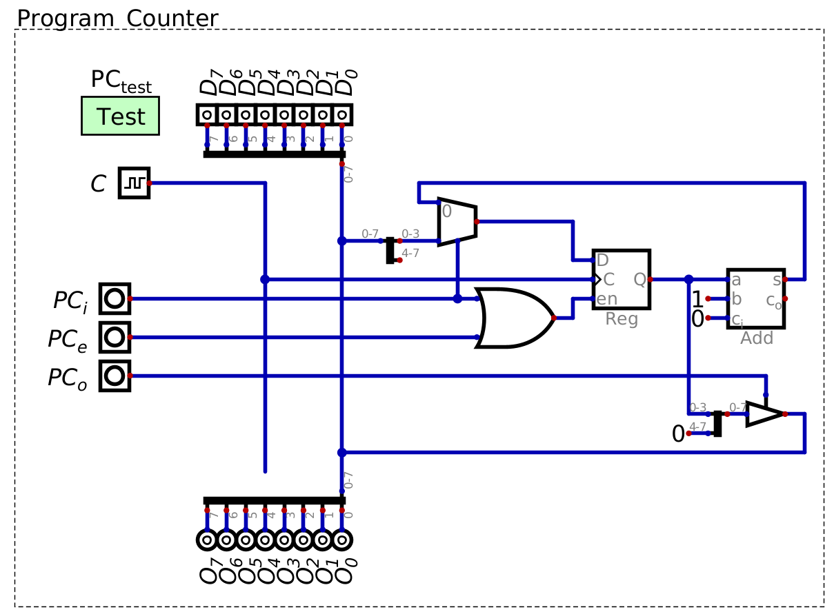
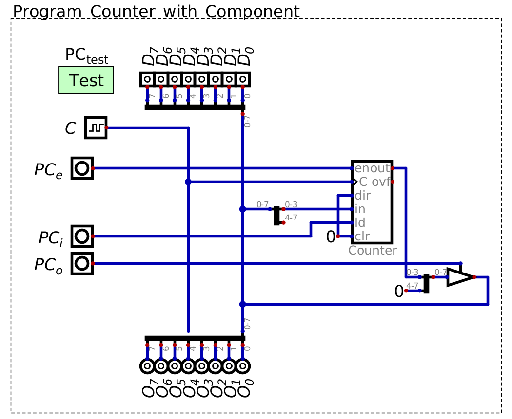
Program counter module with an 8 bit data bus. For the ESAP system, the program counter only needs 4 bits as there
are 16 RAM addresses, therefore splitters/mergers are used to have the program counter interface with the bus.
Due to ESAP’s design, only 4 bits are used to index RAM
The least significant 4 bits on the bus
Since the program counter is keeping track of memory addresses, the program counter only needs to manage 4 bits
Therefore, some mechanism to interface between the two bit lengths is needed
Here, splitters/mergers are used to fit the 4 bit program counter into the 8 bit design
Data from the bus is split
Only the least significant 4 bits are connected to the program counter’s register
Data to the bus is merged with zeros
To pad the counter’s 4 bit output to be a full 8 bits
Like before, the numbers 15 and 4 will be added together, but this time
All data will be preloaded into RAM
Data will not be entered into the system via the data input toggles
The program counter will be used to track of the memory address of the data needing to be retrieved
Although the data input toggles will not be used, the control logic toggles will still need to be controlled
A hex file containing the data for the numbers 15 and 4 will be created
v2.0 raw
0x0F
0x04
This file can then be loaded into RAM
Note
Loading data into RAM before runtime in Digital works a little different compared to the look up tables.
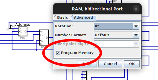
First, the RAM component needs to be marked as “Program Memory”.
“Program Memory” option selection under the Advanced tab for a RAM component.
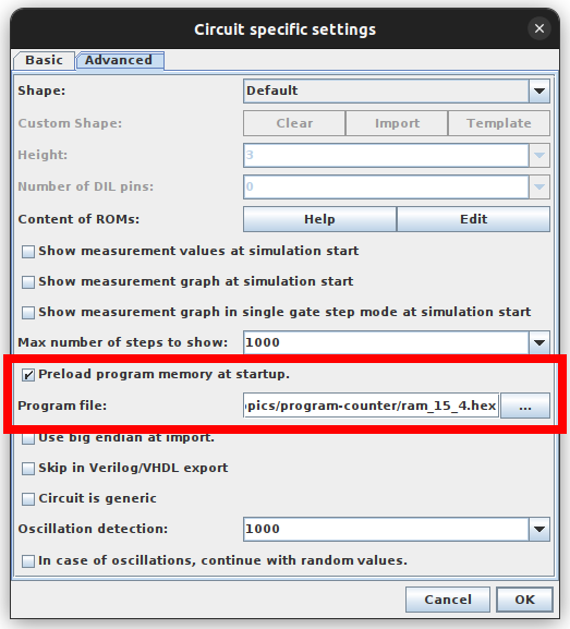
Then, under Digital’s main menu Edit -> Circuit specific settings window, within the Advanced tab, select the
“Preload program memory at startup” option and specify the “Program file” to be loaded.
“Preload program memory at startup” option under the Advanced tab of the circuit specific settings. Notice
the “Program file” is specified.
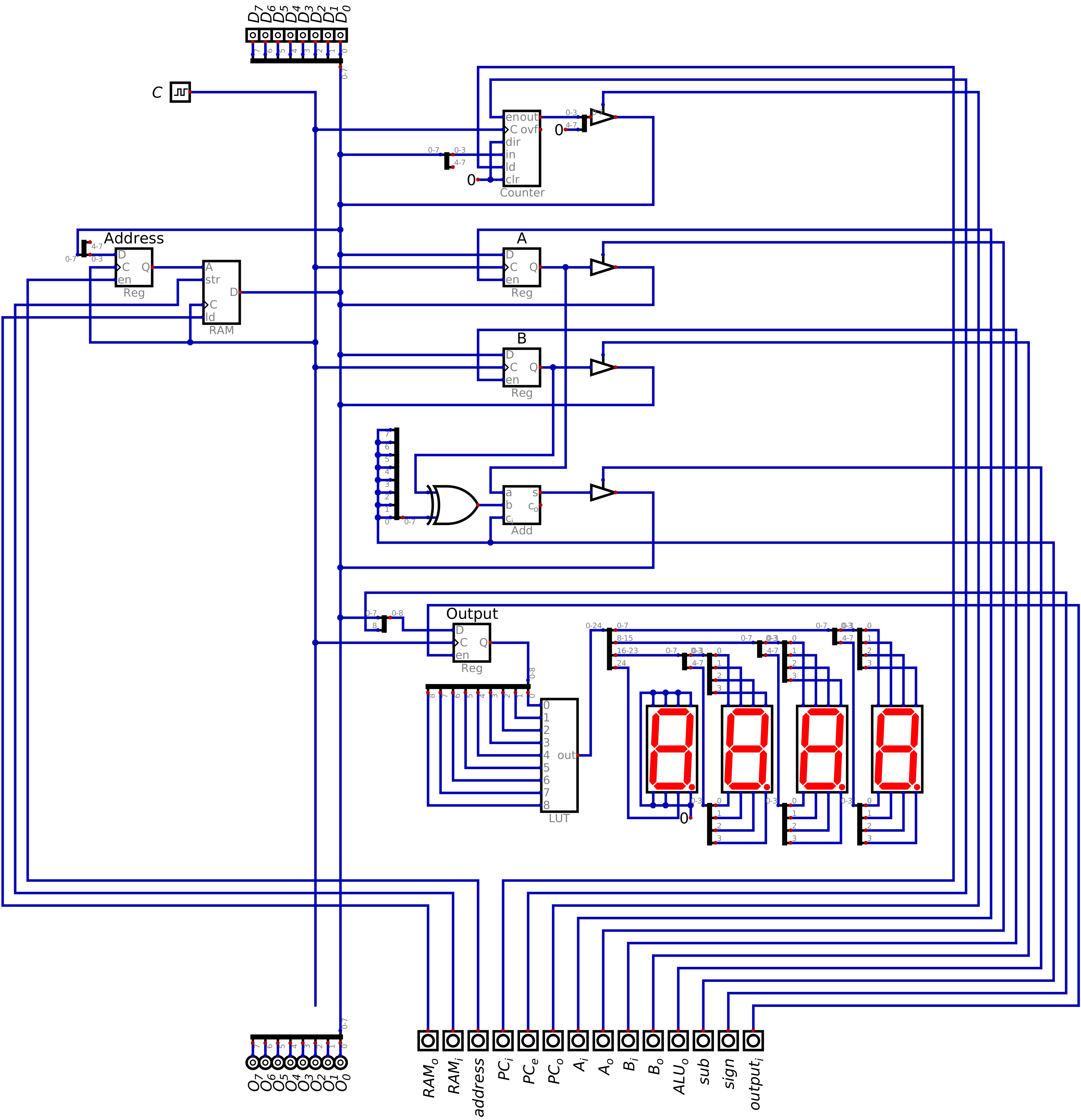
With the data in RAM, think about the steps required to perform the addition
Get the address of the data to be retrieved from the program counter to the address register
Increment the program counter
Remember, the idea is that the program counter always stores the address of the next thing to be dealt with
Output the data from the specified address in RAM to register A
Get the address of the next data to be retrieved from the program counter to the address register
Increment the program counter
Output the data from the specified address in RAM to register B
Perform addition
Put the result of addition into the output register
Below is a table showing how the control lines would be configured to perform the above steps
Like before, each row corresponds to one clock cycle
Due to space limitations, the data and clock columns are removed some control signals’ columns are combined
\(ALU_{o}\) and \(sub\) are combined (alu/sub)
\(Out_{i}\) and \(sign\) are combined (output/sign)
\(PC\) and \(PC_{e}\) are combined (in/out/enable)
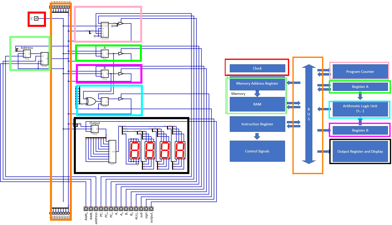
Within Digital it’s possible to combine the steps of (a) program counter -> address register and (b) program counter
enable.
In practice, however, this may be problematic as physical limitations will impact how synchronized the system can
truly be. For example, what if the program counter enable causes the program counter to increment an instant before
the address register can latch? This would cause the wrong value to be latched into the address register.
As previously mentioned, what’s interesting is that no data needed to be input into the system at runtime
This addition happened without needing to manipulate the data input toggles
All the data the system needed was contained within the system
However, the control signals still needed to be manually manipulated with the toggles